SBOSA63A December 2020 – November 2021 LMH32404-Q1
PRODUCTION DATA
- 1 Features
- 2 Applications
- 3 Description
- 4 Revision History
- 5 Pin Configuration and Functions
- 6 Specifications
- 7 Detailed Description
- 8 Application and Implementation
- 9 Power Supply Recommendations
- 10Layout
- 11Device and Documentation Support
- 12Mechanical, Packaging, and Orderable Information
Package Options
Mechanical Data (Package|Pins)
- RHF|28
Thermal pad, mechanical data (Package|Pins)
- RHF|28
Orderable Information
8.1 Application Information
Each differential output pair of the LMH32404-Q1 can directly drive a high-speed differential input ADC. Figure 8-1 shows how the effective signal the effective signal gain between the TIA input and the ADC input is 20 kΩ when driving an ADC with a 100-Ω differential input impedance (RADC_IN = 50 Ω). Equation 2 gives the effective signal gain between the TIA input and the ADC input when driving an ADC with any other value of differential input impedance (RADC_IN ≠ 50 Ω).
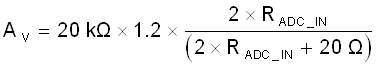
where
- AV = Differential gain from the TIA input to the ADC input
- RADC_IN = Input resistance of the ADC
Figure 8-2 shows that in some designs a matching resistor network can be inserted between the LMH32404-Q1 output and the ADC inputs. Equation 3 gives the effective gain from the TIA input to the ADC input when using a matching resistor network.
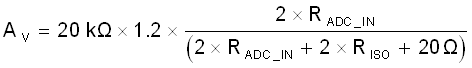
where
- AV = Gain from the TIA input to the ADC input
- RADC_IN = Differential input resistance of the ADC
- RISO = Series resistance between the TIA and ADC
Equation 4 gives the voltage to be applied at the VOD pin (pin 10) if a certain differential offset voltage (VOD) is needed at the ADC input for the circuit in Figure 8-2.
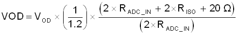
where
- VOD = Voltage applied at pin 10
- VOD = Desired differential offset voltage at the ADC input
- RADC_IN = Differential input resistance of the ADC
- RISO = Series resistance between the TIA and ADC