SNCS103E November 2004 – August 2018 LMH6574
PRODUCTION DATA.
- 1 Features
- 2 Applications
- 3 Description
- 4 Revision History
- 5 Pin Configuration and Functions
- 6 Specifications
- 7 Detailed Description
- 8 Application and Implementation
- 9 Power Supply Recommendations
- 10Layout
- 11Device and Documentation Support
- 12Mechanical, Packaging, and Orderable Information
Package Options
Mechanical Data (Package|Pins)
- D|14
Thermal pad, mechanical data (Package|Pins)
Orderable Information
7.2.4 Driving Capacitive Loads
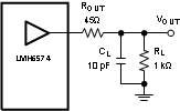
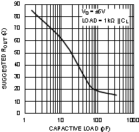
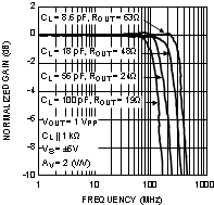
Capacitive output loading applications will benefit from the use of a series output resistor ROUT. Figure 28 shows the use of a series output resistor, ROUT, to stabilize the amplifier output under capacitive loading. Capacitive loads of 5 to 120 pF are the most critical, causing ringing, frequency response peaking and possible oscillation. Figure 29 provides a recommended value for selecting a series output resistor for mitigating capacitive loads. The values suggested in the charts are selected for 0.5 dB or less of peaking in the frequency response. This gives a good compromise between settling time and bandwidth. For applications where maximum frequency response is needed and some peaking is tolerable, the value of ROUT can be reduced slightly from the recommended values.
 Figure 28. Decoupling Capacitive Loads
