SNCS103E November 2004 – August 2018 LMH6574
PRODUCTION DATA.
- 1 Features
- 2 Applications
- 3 Description
- 4 Revision History
- 5 Pin Configuration and Functions
- 6 Specifications
- 7 Detailed Description
- 8 Application and Implementation
- 9 Power Supply Recommendations
- 10Layout
- 11Device and Documentation Support
- 12Mechanical, Packaging, and Orderable Information
Package Options
Mechanical Data (Package|Pins)
- D|14
Thermal pad, mechanical data (Package|Pins)
Orderable Information
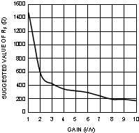
7.2.2 Feedback Resistor Selection
 Figure 27. Suggested RF vs Gain
 The LMH6574 has a current feedback output buffer with gain determined by external feedback (RF) and gain set (RG) resistors. With current feedback amplifiers, the closed loop frequency response is a function of RF. For a gain of 2 V/V, the recommended value of RF is 575Ω. For other gains see Figure 27. Generally, lowering RF from the recommended value will peak the frequency response and extend the bandwidth while increasing the value of RF will cause the frequency response to roll off faster. Reducing the value of RF too far below the recommended value will cause overshoot, ringing and, eventually, oscillation.
Since all applications are slightly different it is worth some experimentation to find the optimal RF for a given circuit. For more information see Current Feedback Loop Gain Analysis and Performance Enhancement, Application Note OA-13 (SNOA366), which describes the relationship between RF and closed-loop frequency response for current feedback operational amplifiers. The impedance looking into pin 12 is approximately 20Ω. This allows for good bandwidth at gains up to 10 V/V. When used with gains over 10 V/V, the LMH6574 will exhibit a “gain bandwidth product” similar to a typical voltage feedback amplifier. For gains of over 10 V/V consider selecting a high performance video amplifier like the LMH6720 (SNOSA39) to provide additional gain.