SNOSA42G November 2002 – December 2014 LMH6624 , LMH6626
PRODUCTION DATA.
- 1 Features
- 2 Applications
- 3 Description
- 4 Revision History
- 5 Pin Configuration and Functions
- 6 Specifications
- 7 Detailed Description
- 8 Application and Implementation
- 9 Power Supply Recommendations
- 10Layout
- 11Device and Documentation Support
- 12Mechanical, Packaging, and Orderable Information
Package Options
Mechanical Data (Package|Pins)
Thermal pad, mechanical data (Package|Pins)
Orderable Information
1 Features
- VS = ±6 V, TA = 25°C, AV = 20 (Typical Values Unless Specified)
- Gain Bandwidth (LMH6624) 1.5 GHz
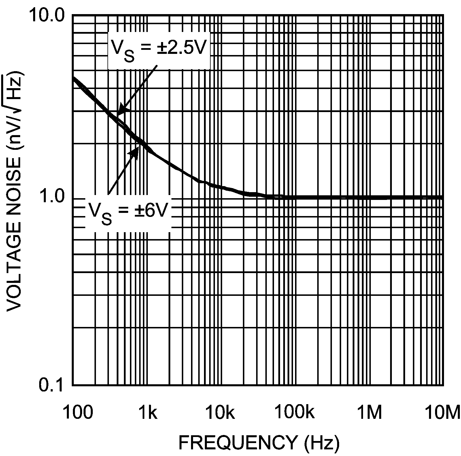
- Input Voltage Noise 0.92 nV/√Hz
- Input Offset Voltage (limit over temp) 700 µV
- Slew Rate 350 V/μs
- Slew Rate (AV = 10) 400 V/μs
- HD2 at f = 10 MHz, RL = 100 Ω −63 dBc
- HD3 at f = 10 MHz, RL = 100 Ω −80 dBc
- Supply Voltage Range (Dual Supply) 2.5 V to 6 V
- Supply Voltage Range (Single Supply) 5 V to 12 V
- Improved Replacement for the CLC425 (LMH6624)
- Stable for Closed Loop |AV| ≥ 10
2 Applications
- Instrumentation Sense Amplifiers
- Ultrasound Pre-amps
- Magnetic Tape & Disk Pre-amps
- Wide Band Active Filters
- Professional Audio Systems
- Opto-electronics
- Medical Diagnostic Systems
3 Description
The LMH6624 and LMH6626 devices offer wide bandwidth (1.5 GHz for single, 1.3 GHz for dual) with very low input noise (0.92 nV/√Hz, 2.3 pA/√Hz) and ultra-low dc errors (100 μV VOS, ±0.1 μV/°C drift) providing very precise operational amplifiers with wide dynamic range. This enables the user to achieve closed-loop gains of greater than 10, in both inverting and non-inverting configurations.
The LMH6624 (single) and LMH6626 (dual) traditional voltage feedback topology provide the following benefits: balanced inputs, low offset voltage and offset current, very low offset drift, 81dB open loop gain, 95dB common mode rejection ratio, and 88dB power supply rejection ratio.
The LMH6624 and LMH6626 devices operate from ±2.5 V to ±6 V in dual supply mode and from 5 V to 12 V in single supply configuration.
LMH6624 is offered in SOT-23-5 and SOIC-8 packages. The LMH6626 is offered in SOIC-8 and VSSOP-8 packages.
Device Information(1)
| PART NUMBER | PACKAGE | BODY SIZE (NOM) |
|---|---|---|
| LMH6624 | SOT-23 (5) | 2.90 mm × 1.60 mm |
| SOIC (8) | 4.90 mm × 3.91 mm | |
| LMH6626 | SOIC (8) | 4.90 mm × 3.91 mm |
| VSSOP (8) | 3.00 mm × 3.00 mm |
- For all available packages, see the orderable addendum at the end of the datasheet.
Voltage Noise vs. Frequency