SNOSA42G November 2002 – December 2014 LMH6624 , LMH6626
PRODUCTION DATA.
- 1 Features
- 2 Applications
- 3 Description
- 4 Revision History
- 5 Pin Configuration and Functions
- 6 Specifications
- 7 Detailed Description
- 8 Application and Implementation
- 9 Power Supply Recommendations
- 10Layout
- 11Device and Documentation Support
- 12Mechanical, Packaging, and Orderable Information
Package Options
Mechanical Data (Package|Pins)
Thermal pad, mechanical data (Package|Pins)
Orderable Information
8 Application and Implementation
NOTE
Information in the following applications sections is not part of the TI component specification, and TI does not warrant its accuracy or completeness. TI’s customers are responsible for determining suitability of components for their purposes. Customers should validate and test their design implementation to confirm system functionality.
8.1 Application Information
A Transimpedance amplifier is used to convert the small output current of a photodiode to a voltage, while maintaining a near constant voltage across the photodiode to minimize non-linearity. Extracting the small signal requires high gain and a low noise amplifier, and therefore, the LMH6624 and LMH6626 devices are ideal for such an application in order to maximize SNR. Furthermore, because of the large gain (RF value) needed, the device used must be high speed so that even with high noise gain (due to the interaction of the feedback resistor and photodiode capacitance), bandwidth is not heavily impacted.
Figure 47 implements a high-speed, single supply, low-noise Transimpedance amplifier commonly used with photo-diodes. The transimpedance gain is set by RF.
8.2 Typical Application
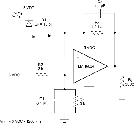 Figure 57. LMH6624 Application Schematic
8.2.1 Design Requirements
Figure 58 shows the Noise Gain (NG) and transfer function (I-V Gain). As with most Transimpedance amplifiers, it is required to compensate for the additional phase lag (Noise Gain zero at fZ) created by the total input capacitance: CD (diode capacitance) + CCM (LMH6624 CM input capacitance) + CDIFF (LMH6624 DIFF input capacitance) looking into RF. This is accomplished by placing CF across RF to create enough phase lead (Noise Gain pole at fP) to stabilize the loop.
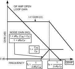 Figure 58. Transimpedance Amplifier Noise Gain and Transfer Function
8.2.2 Detailed Design Procedure
The optimum value of CF is given by Equation 8 resulting in the I-V -3dB bandwidth shown in Equation 9, or around 124 MHz in this case, assuming GBWP = 1.5 GHz, CCM (LMH6624 CM input capacitance) = 0.9 pF, and CDIFF (LMH6624 DIFF input capacitance) = 2 pF. This CF value is a “starting point” and CF needs to be tuned for the particular application as it is often less than 1 pF and thus is easily affected by board parasitics.
Optimum CF Value:

Resulting -3dB Bandwidth:

Equation 10 provides the total input current noise density (ini) equation for the basic Transimpedance configuration and is plotted against feedback resistance (RF) showing all contributing noise sources in Figure 59. The plot indicates the expected total equivalent input current noise density (ini) for a given feedback resistance (RF). This is depicted in the schematic of Figure 60 where total equivalent current noise density (ini) is shown at the input of a noiseless amplifier and noiseless feedback resistor (RF). The total equivalent output voltage noise density (eno) is ini*RF. Noise Equation for Transimpedance Amplifier:
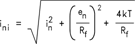
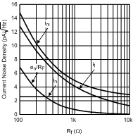 Figure 59. Current Noise Density vs. Feedback Resistance
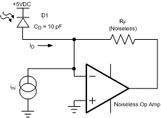 Figure 60. Transimpedance Amplifier Equivalent Input Source Mode
From Figure 61, it is clear that with the LMH6624 extremely low-noise characteristics, for RF < 3 kΩ, the noise performance is entirely dominated by RF thermal noise. Only above this RF threshold, the input noise current (in) of LMH6624 becomes a factor and at no RF setting does the LMH6624 input noise voltage play a significant role. This noise analysis has ignored the possible noise gain increase, due to photo-diode capacitance, at higher frequencies.
8.2.3 Application Curve
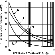 Figure 61. Current Noise Density vs. Feedback Resistance