SBOS964 December   2019 LMH9226

PRODUCTION DATA.  

  1. Features
  2. Applications
  3. Description
    1.     Device Images
      1.      LMH9226: 2.3-GHz to 2.9-GHz Single-Ended Input to Differential Output RF Gain Block Amplifier
  4. Revision History
  5. Pin Configuration and Functions
    1.     Pin Functions
  6. Specifications
    1. 6.1 Absolute Maximum Ratings
    2. 6.2 ESD Ratings
    3. 6.3 Recommended Operating Conditions
    4. 6.4 Thermal Information
    5. 6.5 Electrical Characteristics
    6. 6.6 Typical Characteristics
  7. Detailed Description
    1. 7.1 Overview
    2. 7.2 Functional Block Diagram
    3. 7.3 Feature Description
    4. 7.4 Device Functional Modes
  8. Application and Implementation
    1. 8.1 Application Information
    2. 8.2 Typical Application
      1. 8.2.1 Design Requirements
      2. 8.2.2 Detailed Design Procedure
      3. 8.2.3 Application Curves
  9. Power Supply Recommendations
  10. 10Layout
    1. 10.1 Layout Guidelines
    2. 10.2 Layout Example
  11. 11Device and Documentation Support
    1. 11.1 Documentation Support
      1. 11.1.1 Related Documentation
    2. 11.2 Receiving Notification of Documentation Updates
    3. 11.3 Community Resources
    4. 11.4 Trademarks
    5. 11.5 Electrostatic Discharge Caution
    6. 11.6 Glossary
  12. 12Mechanical, Packaging, and Orderable Information

Package Options

Mechanical Data (Package|Pins)
Thermal pad, mechanical data (Package|Pins)
Orderable Information

Typical Characteristics

at TA = 25°C, VDD = 3.3 V, center frequency (fIN) = 2.6 GHz, single-ended input impedance (ZIN) = 50 Ω, differential output impedance (ZLOAD) = 50 Ω, and POUT(TOTAL) = 8 dBm into ZLOAD = 50 Ω (unless otherwise noted)
LMH9226 D011_LMH9226.gif
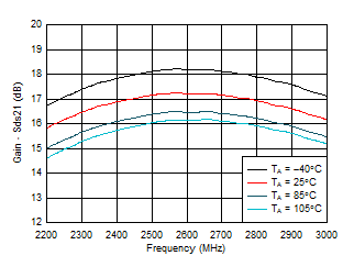
POUT = 2 dBm
Figure 1. Gain vs Frequency and Temperature
LMH9226 D013_LMH9226.gif
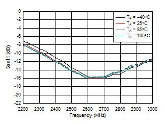
Figure 3. Input Return Loss vs Frequency
LMH9226 D015_LMH9226.gif
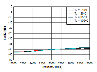
Figure 5. Reverse Isolation vs Frequency
LMH9226 D002_LMH9226.gif
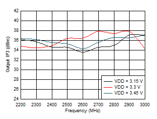
POUT/TONE = 2 dBm, ±1-MHz tone spacing
Figure 7. Output IP3 vs Frequency and Supply Voltage
LMH9226 D004_LMH9226.gif
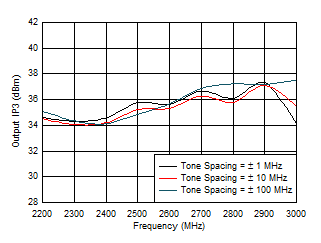
POUT/TONE = 2 dBm
Figure 9. Output IP3 vs Frequency and Tone Spacing
LMH9226 D006_LMH9226.gif
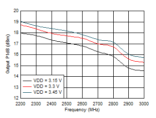
Figure 11. Output P1dB vs Frequency and Supply Voltage
LMH9226 D008_LMH9226.gif
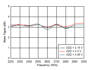
ZSOURCE = 50 Ω
Figure 13. Noise Figure vs Frequency and Supply Voltage
LMH9226 D017_LMH9226.gif
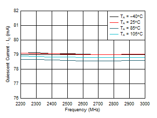
Figure 15. Quiescent Current vs Frequency and Temperature
LMH9226 D010_LMH9226.gif
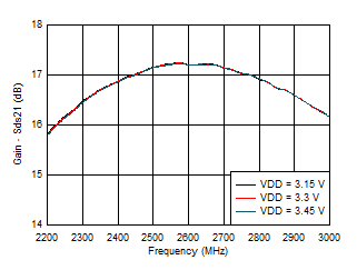
POUT = 2 dBm
Figure 2. Gain vs Frequency and Supply Voltage
LMH9226 D014_LMH9226.gif
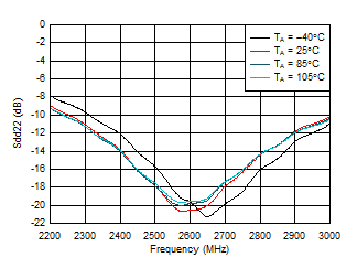
Figure 4. Output Return Loss vs Frequency
LMH9226 D001_LMH9226.gif
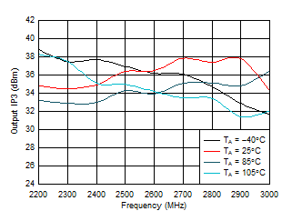
POUT/TONE = 2 dBm, ±1-MHz tone spacing
Figure 6. Output IP3 vs Frequency and Temperature
LMH9226 D003_LMH9226.gif
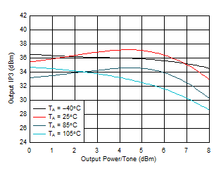
f = 2.6 GHz, ±1-MHz tone spacing
Figure 8. Output IP3 vs Output Power per Tone
LMH9226 D005_LMH9226.gif
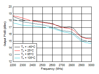
Figure 10. Output P1dB vs Frequency and Temperature
LMH9226 D007_LMH9226.gif
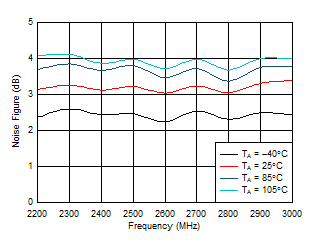
ZSOURCE = 50 Ω
Figure 12. Noise Figure vs Frequency and Temperature
LMH9226 D009_LMH9226.gif
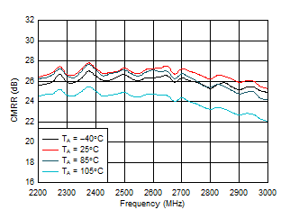
Figure 14. CMRR vs Frequency
LMH9226 D018_LMH9226.gif
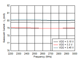
Figure 16. Quiescent Current vs Frequency and Supply Voltage