SNAS512J september   2011  – may 2023 LMK00301

PRODUCTION DATA  

  1.   1
  2. Features
  3. Applications
  4. Description
  5. Revision History
  6. Device Comparison
  7. Pin Configuration and Functions
  8. Specifications
    1. 7.1 Absolute Maximum Ratings
    2. 7.2 ESD Ratings
    3. 7.3 Recommended Operating Conditions
    4. 7.4 Thermal Information
    5. 7.5 Electrical Characteristics
    6. 7.6 Typical Characteristics
  9. Parameter Measurement Information
    1. 8.1 Differential Voltage Measurement Terminology
  10. Detailed Description
    1. 9.1 Overview
    2. 9.2 Functional Block Diagram
    3. 9.3 Feature Description
      1. 9.3.1 VCC and VCCO Power Supplies
    4. 9.4 Device Functional Modes
      1. 9.4.1 Clock Inputs
      2. 9.4.2 Clock Outputs
        1. 9.4.2.1 Reference Output
  11. 10Application and Implementation
    1. 10.1 Application Information
    2. 10.2 Typical Application
      1. 10.2.1 Design Requirements
        1. 10.2.1.1 Driving the Clock Inputs
        2. 10.2.1.2 Crystal Interface
      2. 10.2.2 Detailed Design Procedure
        1. 10.2.2.1 Termination and Use of Clock Drivers
          1. 10.2.2.1.1 Termination for DC Coupled Differential Operation
          2. 10.2.2.1.2 Termination for AC Coupled Differential Operation
          3. 10.2.2.1.3 Termination for Single-Ended Operation
      3. 10.2.3 Application Curves
  12. 11Power Supply Recommendations
    1. 11.1 Power Supply Sequencing
    2. 11.2 Current Consumption and Power Dissipation Calculations
      1. 11.2.1 Power Dissipation Example #1: Separate VCC and VCCO Supplies with Unused Outputs
      2. 11.2.2 Power Dissipation Example #2: Worst-Case Dissipation
    3. 11.3 Power Supply Bypassing
      1. 11.3.1 Power Supply Ripple Rejection
    4. 11.4 Thermal Management
  13. 12Layout
    1. 12.1 Layout Guidelines
    2. 12.2 Layout Example
  14. 13Device and Documentation Support
    1. 13.1 Documentation Support
      1. 13.1.1 Related Documentation
    2. 13.2 Receiving Notification of Documentation Updates
    3. 13.3 Support Resources
    4. 13.4 Trademarks
    5. 13.5 Electrostatic Discharge Caution
    6. 13.6 Glossary
  15. 14Mechanical, Packaging, and Orderable Information

Package Options

Mechanical Data (Package|Pins)
Thermal pad, mechanical data (Package|Pins)
Orderable Information

Description

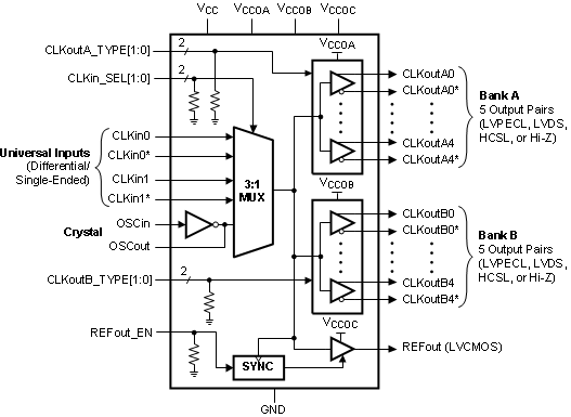
The LMK00301 is a 3-GHz, 10-output differential fanout buffer intended for high-frequency, low-jitter clock and data distribution, and level translation. The input clock can be selected from two universal inputs or one crystal input. The selected input clock is distributed to two banks of five differential outputs and one LVCMOS output. Both differential output banks can be independently configured as LVPECL, LVDS, or HCSL drivers, or disabled. The LVCMOS output has a synchronous enable input for runt-pulse-free operation when enabled or disabled. The LMK00301 operates from a 3.3-V core supply and three independent 3.3-V or 2.5-V output supplies.

The LMK00301 provides high performance, versatility, and power efficiency, making it ideal for replacing fixed-output buffer devices while increasing timing margin in the system. The LMK00301 offers a design spin, the LMK00301A, that does not have power supply sequencing requirements between the core and output supply domains.

Package Information(1)
PART NUMBER PACKAGE PACKAGE SIZE (NOM)
LMK00301(2) WQFN (48) 7.00 mm × 7.00 mm
For all available packages, see the orderable addendum at the end of the data sheet.
The LMK00301A is a design spin available as an orderable in orderable addendum at the end of the data sheet.
GUID-E01E603D-9609-4C67-BBA1-B4DE5DA10FC5-low.gif Functional Block Diagram