SNAS578D February 2012 – March 2016 LMK00306
PRODUCTION DATA.
- 1 Features
- 2 Applications
- 3 Description
- 4 Revision History
- 5 Pin Configuration and Functions
- 6 Specifications
- 7 Parameter Measurement Information
- 8 Detailed Description
- 9 Application and Implementation
- 10Power Supply Recommendations
- 11Device and Documentation Support
- 12Mechanical, Packaging, and Orderable Information
Package Options
Refer to the PDF data sheet for device specific package drawings
Mechanical Data (Package|Pins)
- NJK|36
Thermal pad, mechanical data (Package|Pins)
Orderable Information
6 Specifications
6.1 Absolute Maximum Ratings
over operating free-air temperature range (unless otherwise noted) (1)(2)| MIN | MAX | UNIT | ||
|---|---|---|---|---|
| VCC, VCCO | Supply Voltages | -0.3 | 3.6 | V |
| VIN | Input Voltage | -0.3 | (VCC + 0.3) | V |
| TSTG | Storage Temperature | -65 | +150 | °C |
| TL | Lead Temperature (solder 4 s) | +260 | °C | |
| TJ | Junction Temperature | +150 | °C |
(1) Stresses beyond those listed under Absolute Maximum Ratings may cause permanent damage to the device. These are stress ratings only, which do not imply functional operation of the device at these or any other conditions beyond those indicated under Recommended Operating Conditions. Exposure to absolute-maximum-rated conditions for extended periods may affect device reliability.
(2) If Military/Aerospace specified devices are required, please contact the Texas Instruments Sales Office/Distributors for availability and specifications.
6.2 ESD Ratings
| VALUE | UNIT | |||
|---|---|---|---|---|
| V(ESD) | Electrostatic discharge | Human-body model (HBM), per ANSI/ESDA/JEDEC JS-001(1) | ±2000 | V |
| Machine model (MM) | ±150 | |||
| Charged-device model (CDM), per JEDEC specification JESD22-C101(2) | ±750 | |||
(1) JEDEC document JEP155 states that 500-V HBM allows safe manufacturing with a standard ESD control process. Manufacturing with less than 500-V HBM is possible with the necessary precautions. Pins listed as ±2000 V may actually have higher performance.
(2) JEDEC document JEP157 states that 250-V CDM allows safe manufacturing with a standard ESD control process. Manufacturing with less than 250-V CDM is possible with the necessary precautions. Pins listed as ±750 V may actually have higher performance.
6.3 Recommended Operating Conditions
| PARAMETER | MIN | TYP | MAX | UNIT | |
|---|---|---|---|---|---|
| TA | Ambient Temperature Range | -40 | 25 | 85 | °C |
| TJ | Junction Temperature | 125 | °C | ||
| VCC | Core Supply Voltage Range | 3.15 | 3.3 | 3.45 | V |
| VCCO | Output Supply Voltage Range (1)(2) | 3.3 – 5% 2.5 – 5% |
3.3 2.5 |
3.3 + 5% 2.5 + 5% |
V |
(1) The output supply voltages or pins (VCCOA, VCCOB, and VCCOC) will be called VCCO in general when no distinction is needed, or when the output supply can be inferred from the output bank/type.
(2) Vcco should be less than or equal to Vcc (Vcco ≤ Vcc).
6.4 Thermal Information
| THERMAL METRIC(1)(2) | NJK0036A (WQFN) |
UNIT | |
|---|---|---|---|
| 36 PINS | |||
| RθJA | Junction-to-ambient thermal resistance | 31.8 | °C/W |
| RθJC(top) (DAP) | Junction-to-case (top) thermal resistance | 7.2 | |
(1) For more information about traditional and new thermal metrics, see the IC Package Thermal Metrics application report, SPRA953.
(2) Specification assumes 9 thermal vias connect the die attach pad (DAP) to the embedded copper plane on the 4-layer JEDEC board. These vias play a key role in improving the thermal performance of the package. It is recommended that the maximum number of vias be used in the board layout.
6.5 Electrical Characteristics
Unless otherwise specified: Vcc = 3.3 V ± 5%, Vcco = 3.3 V ± 5%, 2.5 V ± 5%, -40 °C ≤ TA ≤ 85 °C, CLKin driven differentially, input slew rate ≥ 3 V/ns. Typical values represent most likely parametric norms at Vcc = 3.3 V, Vcco = 3.3 V, TA = 25 °C, and at the Recommended Operation Conditions at the time of product characterization and are not ensured. (1)(1)| PARAMETER | TEST CONDITIONS | MIN | TYP | MAX | UNIT | ||
|---|---|---|---|---|---|---|---|
| CURRENT CONSUMPTION(2) | |||||||
| ICC_CORE | Core Supply Current, All Outputs Disabled | CLKinX selected | 8.5 | 10.5 | mA | ||
| OSCin selected | 10 | 13.5 | mA | ||||
| ICC_PECL | Additive Core Supply Current, Per LVPECL Bank Enabled | 20 | 26.5 | mA | |||
| ICC_LVDS | Additive Core Supply Current, Per LVDS Bank Enabled | 24 | 29.5 | mA | |||
| ICC_HCSL | Additive Core Supply Current, Per HCSL Bank Enabled | 29 | 35 | mA | |||
| ICC_CMOS | Additive Core Supply Current, LVCMOS Output Enabled | 3.5 | 5.5 | mA | |||
| ICCO_PECL | Additive Output Supply Current, Per LVPECL Bank Enabled | Includes Output Bank Bias and Load Currents, RT = 50 Ω to Vcco - 2V on all outputs in bank |
100 | 123 | mA | ||
| ICCO_LVDS | Additive Output Supply Current, Per LVDS Bank Enabled | 20 | 27.5 | mA | |||
| ICCO_HCSL | Additive Output Supply Current, Per HCSL Bank Enabled | Includes Output Bank Bias and Load Currents, RT = 50 Ω on all outputs in bank |
50 | 65 | mA | ||
| ICCO_CMOS | Additive Output Supply Current, LVCMOS Output Enabled | 200 MHz, CL = 5 pF | Vcco = 3.3 V ± 5% | 9 | 10 | mA | |
| Vcco = 2.5 V ± 5% | 7 | 8 | mA | ||||
| POWER SUPPLY RIPPLE REJECTION (PSRR) | |||||||
| PSRRPECL | Ripple-Induced Phase Spur Level Differential LVPECL Output(3) | 100 kHz, 100 mVpp Ripple Injected on Vcco, Vcco = 2.5 V | 156.25 MHz | -65 | dBc | ||
| 312.5 MHz | -63 | ||||||
| PSRRLVDS | Ripple-Induced Phase Spur Level Differential LVDS Output(3) | 156.25 MHz | -76 | dBc | |||
| 312.5 MHz | -74 | ||||||
| PSRRHCSL | Ripple-Induced Phase Spur Level Differential HCSL Output(3) | 156.25 MHz | -72 | dBc | |||
| 312.5 MHz | -63 | ||||||
| CMOS CONTROL INPUTS (CLKin_SELn, CLKoutX_TYPEn, REFout_EN) | |||||||
| VIH | High-Level Input Voltage | 1.6 | Vcc | V | |||
| VIL | Low-Level Input Voltage | GND | 0.4 | V | |||
| IIH | High-Level Input Current | VIH = Vcc, Internal pull-down resistor | 50 | µA | |||
| IIL | Low-Level Input Current | VIL = 0 V, Internal pull-down resistor | -5 | 0.1 | µA | ||
| CLOCK INPUTS (CLKin0/CLKin0*, CLKin1/CLKin1*) | |||||||
| fCLKin | Input Frequency Range(10) | Functional up to 3.1 GHz Output frequency range and timing specified per output type (refer to LVPECL, LVDS, HCSL, LVCMOS output specifications) |
DC | 3.1 | GHz | ||
| VIHD | Differential Input High Voltage | CLKin driven differentially | Vcc | V | |||
| VILD | Differential Input Low Voltage | GND | V | ||||
| VID | Differential Input Voltage Swing(4) | 0.15 | 1.3 | V | |||
| VCMD | Differential Input Common Mode Voltage | VID = 150 mV | 0.25 | Vcc - 1.2 | V | ||
| VID = 350 mV | 0.25 | Vcc - 1.1 | |||||
| VID = 800 mV | 0.25 | Vcc -0.9 | |||||
| VIH | Single-Ended Input High Voltage | CLKinX driven single-ended (AC or DC coupled), CLKinX* AC coupled to GND or externally biased within VCM range | Vcc | V | |||
| VIL | Single-Ended Input Low Voltage | GND | V | ||||
| VI_SE | Single-Ended Input Voltage Swing(15)(17) | 0.3 | 2 | Vpp | |||
| VCM | Single-Ended Input Common Mode Voltage | 0.25 | Vcc - 1.2 | V | |||
| ISOMUX | Mux Isolation, CLKin0 to CLKin1 | fOFFSET > 50 kHz, PCLKinX = 0 dBm | fCLKin0 = 100 MHz | -84 | dBc | ||
| fCLKin0 = 200 MHz | -82 | ||||||
| fCLKin0 = 500 MHz | -71 | ||||||
| fCLKin0 = 1000 MHz | -65 | ||||||
| CRYSTAL INTERFACE (OSCin, OSCout) | |||||||
| FCLK | External Clock Frequency Range(10) | OSCin driven single-ended, OSCout floating | 250 | MHz | |||
| FXTAL | Crystal Frequency Range | Fundamental mode crystal ESR ≤ 200 Ω (10 to 30 MHz) ESR ≤ 125 Ω (30 to 40 MHz)(5) |
10 | 40 | MHz | ||
| CIN | OSCin Input Capacitance | 4 | pF | ||||
| LVPECL OUTPUTS (CLKoutAn/CLKoutAn*, CLKoutBn/CLKoutBn*) | |||||||
| fCLKout_FS | Maximum Output Frequency Full VOD Swing(10)(11) |
VOD ≥ 600 mV, RL = 100 Ω differential |
Vcco = 3.3 V ± 5%, RT = 160 Ω to GND |
1.0 | 1.2 | GHz | |
| Vcco = 2.5 V ± 5%, RT = 91 Ω to GND |
0.75 | 1.0 | |||||
| fCLKout_RS | Maximum Output Frequency Reduced VOD Swing(10)(11) |
VOD ≥ 400 mV, RL = 100 Ω differential |
Vcco = 3.3 V ± 5%, RT = 160 Ω to GND |
1.5 | 3.1 | GHz | |
| Vcco = 2.5 V ± 5%, RT = 91 Ω to GND |
1.5 | 2.3 | |||||
| JitterADD | Additive RMS Jitter, Integration Bandwidth 10 kHz to 20 MHz(10)(6)(16) |
Vcco = 2.5 V ± 5%: RT = 91 Ω to GND, Vcco = 3.3 V ± 5%: RT = 160 Ω to GND, RL = 100 Ω differential |
CLKin: 100 MHz, Slew rate ≥ 3 V/ns |
77 | 98 | fs | |
| CLKin: 156.25 MHz, Slew rate ≥ 3 V/ns |
54 | 78 | |||||
| JitterADD | Additive RMS Jitter Integration Bandwidth 1 MHz to 20 MHz(6) |
Vcco = 3.3 V, RT = 160 Ω to GND, RL = 100 Ω differential |
CLKin: 100 MHz, Slew rate ≥ 3 V/ns |
59 | fs | ||
| CLKin: 156.25 MHz, Slew rate ≥ 2.7 V/ns | 64 | ||||||
| CLKin: 625 MHz, Slew rate ≥ 3 V/ns |
30 | ||||||
| JitterADD | Additive RMS Jitter with LVPECL clock source from LMK03806(6)(7) | Vcco = 3.3 V, RT = 160 Ω to GND, RL = 100 Ω differential |
CLKin: 156.25 MHz, JSOURCE = 190 fs RMS (10 kHz to 1 MHz) | 20 | fs | ||
| CLKin: 156.25 MHz, JSOURCE = 195 fs RMS (12 kHz to 20 MHz) | 51 | ||||||
| Noise Floor | Noise Floor fOFFSET ≥ 10 MHz(8)(9) |
Vcco = 3.3 V, RT = 160 Ω to GND, RL = 100 Ω differential |
CLKin: 100 MHz, Slew rate ≥ 3 V/ns |
-162.5 | dBc/Hz | ||
| CLKin: 156.25 MHz, Slew rate ≥ 2.7 V/ns | -158.1 | ||||||
| CLKin: 625 MHz, Slew rate ≥ 3 V/ns |
-154.4 | ||||||
| DUTY | Duty Cycle(10) | 50% input clock duty cycle | 45% | 55% | |||
| VOH | Output High Voltage | TA = 25 °C, DC Measurement, RT = 50 Ω to Vcco - 2 V |
Vcco - 1.2 | Vcco - 0.9 | Vcco - 0.7 | V | |
| VOL | Output Low Voltage | Vcco - 2.0 | Vcco - 1.75 | Vcco - 1.5 | V | ||
| VOD | Output Voltage Swing(4) | 600 | 830 | 1000 | mV | ||
| tR | Output Rise Time 20% to 80%(15) |
RT = 160 Ω to GND, Uniform transmission line up to 10 in. with 50-Ω characteristic impedance, RL = 100 Ω differential,CL ≤ 5 pF |
175 | 300 | ps | ||
| tF | Output Fall Time 80% to 20%(15) |
175 | 300 | ps | |||
| LVDS OUTPUTS (CLKoutAn/CLKoutAn*, CLKoutBn/CLKoutBn*) | |||||||
| fCLKout_FS | Maximum Output Frequency Full VOD Swing(10)(11) |
VOD ≥ 250 mV, RL = 100 Ω differential |
1.0 | 1.6 | GHz | ||
| fCLKout_RS | Maximum Output Frequency Reduced VOD Swing(10)(11) |
VOD ≥ 200 mV, RL = 100 Ω differential |
1.5 | 2.1 | GHz | ||
| JitterADD | Additive RMS Jitter, Integration Bandwidth 10 kHz to 20 MHz(10)(6)(16) |
RL = 100 Ω differential | CLKin: 100 MHz, Slew rate ≥ 3 V/ns |
94 | 115 | fs | |
| CLKin: 156.25 MHz, Slew rate ≥ 3 V/ns |
70 | 90 | |||||
| JitterADD | Additive RMS Jitter Integration Bandwidth 1 MHz to 20 MHz(6) |
Vcco = 3.3 V, RL = 100 Ω differential |
CLKin: 100 MHz, Slew rate ≥ 3 V/ns |
89 | fs | ||
| CLKin: 156.25 MHz, Slew rate ≥ 2.7 V/ns |
77 | ||||||
| CLKin: 625 MHz, Slew rate ≥ 3 V/ns |
37 | ||||||
| Noise Floor | Noise Floor fOFFSET ≥ 10 MHz(8)(9) |
Vcco = 3.3 V, RL = 100 Ω differential |
CLKin: 100 MHz, Slew rate ≥ 3 V/ns |
-159.5 | dBc/Hz | ||
| CLKin: 156.25 MHz, Slew rate ≥ 2.7 V/ns |
-157.0 | ||||||
| CLKin: 625 MHz, Slew rate ≥ 3 V/ns |
-152.7 | ||||||
| DUTY | Duty Cycle(10) | 50% input clock duty cycle | 45% | 55% | |||
| VOD | Output Voltage Swing(4) | TA = 25 °C, DC Measurement, RL = 100 Ω differential |
250 | 400 | 450 | mV | |
| ΔVOD | Change in Magnitude of VOD for Complementary Output States | -50 | 50 | mV | |||
| VOS | Output Offset Voltage | 1.125 | 1.25 | 1.375 | V | ||
| ΔVOS | Change in Magnitude of VOS for Complementary Output States | -35 | 35 | mV | |||
| ISA
ISB |
Output Short Circuit Current Single Ended | TA = 25 °C, Single ended outputs shorted to GND |
-24 | 24 | mA | ||
| ISAB | Output Short Circuit Current Differential | Complementary outputs tied together | -12 | 12 | mA | ||
| tR | Output Rise Time 20% to 80%(15) |
Uniform transmission line up to 10 inches with 50-Ω characteristic impedance, RL = 100 Ω differential, CL ≤ 5 pF | 175 | 300 | ps | ||
| tF | Output Fall Time 80% to 20%(15) |
175 | 300 | ps | |||
| HCSL OUTPUTS (CLKoutAn/CLKoutAn*, CLKoutBn/CLKoutBn*) | |||||||
| fCLKout | Output Frequency Range(10) | RL = 50 Ω to GND, CL ≤ 5 pF | DC | 400 | MHz | ||
| JitterADD_PCIe | Additive RMS Phase Jitter for PCIe 3.0(10) | PCIe Gen 3, PLL BW = 2–5 MHz, CDR = 10 MHz |
CLKin: 100 MHz, Slew rate ≥ 0.6 V/ns |
0.03 | 0.15 | ps | |
| JitterADD | Additive RMS Jitter Integration Bandwidth 1 MHz to 20 MHz(6) |
Vcco = 3.3 V, RT = 50 Ω to GND |
CLKin: 100 MHz, Slew rate ≥ 3 V/ns |
77 | fs | ||
| CLKin: 156.25 MHz, Slew rate ≥ 2.7 V/ns |
86 | ||||||
| Noise Floor | Noise Floor fOFFSET ≥ 10 MHz(8)(9) |
Vcco = 3.3 V, RT = 50 Ω to GND |
CLKin: 100 MHz, Slew rate ≥ 3 V/ns |
-161.3 | dBc/Hz | ||
| CLKin: 156.25 MHz, Slew rate ≥ 2.7 V/ns |
-156.3 | ||||||
| DUTY | Duty Cycle(10) | 50% input clock duty cycle | 45% | 55% | |||
| VOH | Output High Voltage | TA = 25 °C, DC Measurement, RT = 50 Ω to GND | 520 | 810 | 920 | mV | |
| VOL | Output Low Voltage | -150 | 0.5 | 150 | mV | ||
| VCROSS | Absolute Crossing Voltage(10)(12) | RL = 50 Ω to GND, CL ≤ 5 pF | 160 | 350 | 460 | mV | |
| ΔVCROSS | Total Variation of VCROSS(10)(12) | 140 | mV | ||||
| tR | Output Rise Time 20% to 80%(15)(12) |
250 MHz, Uniform transmission line up to 10 inches with 50-Ω characteristic impedance, RL = 50 Ω to GND, CL ≤ 5 pF | 300 | 500 | ps | ||
| tF | Output Fall Time 80% to 20%(15)(12) |
300 | 500 | ps | |||
| LVCMOS OUTPUT (REFout) | |||||||
| fCLKout | Output Frequency Range(10) | CL ≤ 5 pF | DC | 250 | MHz | ||
| JitterADD | Additive RMS Jitter Integration Bandwidth 1 MHz to 20 MHz(6) |
Vcco = 3.3 V, CL ≤ 5 pF | 100 MHz, Input Slew rate ≥ 3 V/ns | 95 | fs | ||
| Noise Floor | Noise Floor fOFFSET ≥ 10 MHz(8)(9) |
Vcco = 3.3 V, CL ≤ 5 pF | 100 MHz, Input Slew rate ≥ 3 V/ns | -159.3 | dBc/Hz | ||
| DUTY | Duty Cycle(10) | 50% input clock duty cycle | 45% | 55% | |||
| VOH | Output High Voltage | 1 mA load | Vcco - 0.1 | V | |||
| VOL | Output Low Voltage | 0.1 | V | ||||
| IOH | Output High Current (Source) | Vo = Vcco / 2 | Vcco = 3.3 V | 28 | mA | ||
| Vcco = 2.5 V | 20 | ||||||
| IOL | Output Low Current (Sink) | Vcco = 3.3 V | 28 | mA | |||
| Vcco = 2.5 V | 20 | ||||||
| tR | Output Rise Time 20% to 80%(15)(12) |
250 MHz, Uniform transmission line up to 10 inches with 50-Ω characteristic impedance, RL = 50 Ω to GND, CL ≤ 5 pF | 225 | 400 | ps | ||
| tF | Output Fall Time 80% to 20%(15)(12) |
225 | 400 | ps | |||
| tEN | Output Enable Time(13) | CL ≤ 5 pF | 3 | cycles | |||
| tDIS | Output Disable Time(13) | 3 | cycles | ||||
| PROPAGATION DELAY and OUTPUT SKEW | |||||||
| tPD_PECL | Propagation Delay CLKin-to-LVPECL(15) |
RT = 160 Ω to GND, RL = 100 Ω differential, CL ≤ 5 pF |
180 | 360 | 540 | ps | |
| tPD_LVDS | Propagation Delay CLKin-to-LVDS(15) |
RL = 100 Ω differential, CL ≤ 5 pF | 200 | 400 | 600 | ps | |
| tPD_HCSL | Propagation Delay CLKin-to-HCSL(15)(12) |
RT = 50 Ω to GND, CL ≤ 5 pF | 295 | 590 | 885 | ps | |
| tPD_CMOS | Propagation Delay CLKin-to-LVCMOS(15)(12) |
CL ≤ 5 pF | Vcco = 3.3 V | 900 | 1475 | 2300 | ps |
| Vcco = 2.5 V | 1000 | 1550 | 2700 | ||||
| tSK(O) | Output Skew LVPECL/LVDS/HCSL (10)(12)(14) |
Skew specified between any two CLKouts with the same buffer type. Load conditions per output type are the same as propagation delay specifications. | 30 | 50 | ps | ||
| tSK(PP) | Part-to-Part Output Skew LVPECL/LVDS/HCSL (15)(12)(14) |
80 | 120 | ps | |||
(1) The Electrical Characteristics tables list ensured specifications under the listed Recommended Operating Conditions except as otherwise modified or specified by the Electrical Characteristics Conditions and/or Notes. Typical specifications are estimations only and are not ensured.
(2) See Power Supply Recommendations for more information on current consumption and power dissipation calculations.
(3) Power supply ripple rejection, or PSRR, is defined as the single-sideband phase spur level (in dBc) modulated onto the clock output when a single-tone sinusoidal signal (ripple) is injected onto the Vcco supply. Assuming no amplitude modulation effects and small index modulation, the peak-to-peak deterministic jitter (DJ) can be calculated using the measured single-sideband phase spur level (PSRR) as follows: DJ (ps pk-pk) = [ (2 * 10(PSRR / 20)) / (π * fCLK) ] * 1E12
(4) See Differential Voltage Measurement Terminology for definition of VID and VOD voltages.
(5) The ESR requirements stated must be met to ensure that the oscillator circuitry has no startup issues. However, lower ESR values for the crystal may be necessary to stay below the maximum power dissipation (drive level) specification of the crystal. Refer to Crystal Interface for crystal drive level considerations.
(6) For the 100 MHz and 156.25 MHz clock input conditions, Additive RMS Jitter (JADD) is calculated using Method #1: JADD = SQRT(JOUT2 - JSOURCE2), where JOUT is the total RMS jitter measured at the output driver and JSOURCE is the RMS jitter of the clock source applied to CLKin. For the 625 MHz clock input condition, Additive RMS Jitter is approximated using Method #2: JADD = SQRT(2*10dBc/10) / (2*π*fCLK), where dBc is the phase noise power of the Output Noise Floor integrated from 1 to 20 MHz bandwidth. The phase noise power can be calculated as: dBc = Noise Floor + 10*log10(20 MHz - 1 MHz). The additive RMS jitter was approximated for 625 MHz using Method #2 because the RMS jitter of the clock source was not sufficiently low enough to allow practical use of Method #1. Refer to the “Noise Floor vs. CLKin Slew Rate” and “RMS Jitter vs. CLKin Slew Rate” plots in Typical Characteristics.
(7) 156.25 MHz LVPECL clock source from LMK03806 with 20 MHz crystal reference (crystal part number: ECS-200-20-30BU-DU). JSOURCE = 190 fs RMS (10 kHz to 1 MHz) and 195 fs RMS (12 kHz to 20 MHz). Refer to the LMK03806 datasheet for more information.
(8) The noise floor of the output buffer is measured as the far-out phase noise of the buffer. Typically this offset is ≥ 10 MHz, but for lower frequencies this measurement offset can be as low as 5 MHz due to measurement equipment limitations.
(9) Phase noise floor will degrade as the clock input slew rate is reduced. Compared to a single-ended clock, a differential clock input (LVPECL, LVDS) will be less susceptible to degradation in noise floor at lower slew rates due to its common mode noise rejection. However, it is recommended to use the highest possible input slew rate for differential clocks to achieve optimal noise floor performance at the device outputs.
(11) See Typical Characteristics for output operation over frequency.
(12) AC timing parameters for HCSL or CMOS are dependent on output capacitive loading.
(13) Output Enable Time is the number of input clock cycles it takes for the output to be enabled after REFout_EN is pulled high. Similarly, Output Disable Time is the number of input clock cycles it takes for the output to be disabled after REFout_EN is pulled low. The REFout_EN signal should have an edge transition much faster than that of the input clock period for accurate measurement.
(14) Output skew is the propagation delay difference between any two outputs with identical output buffer type and equal loading while operating at the same supply voltage and temperature conditions.
(15) Parameter is specified by design, not tested in production.
(16) 100 MHz and 156.25 MHz input source from Rohde & Schwarz SMA100A Low-Noise Signal Generator and Sine-to-Square-wave Conversion block.
(17) For clock input frequency ≥ 100 MHz, CLKinX can be driven with single-ended (LVCMOS) input swing up to 3.3 Vpp. For clock input frequency < 100 MHz, the single-ended input swing should be limited to 2 Vpp max to prevent input saturation (refer to Driving the Clock Inputs for interfacing 2.5 V/3.3 V LVCMOS clock input < 100 MHz to CLKinX).
6.6 Typical Characteristics
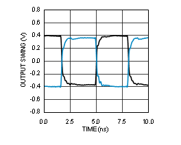
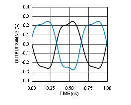
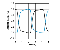
Unless otherwise specified: Vcc = 3.3 V, Vcco = 3.3 V, TA = 25 °C, CLKin driven differentially, input slew rate ≥ 3 V/ns. Consult Table 1 at the end of Typical Characteristics for graph footnotes.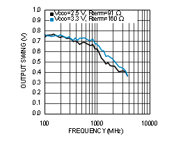
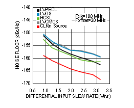
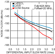
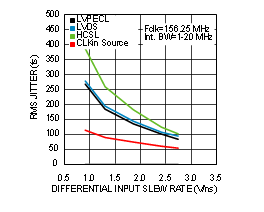
| See Note 1 in Graph Notes | ||
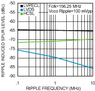
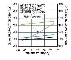
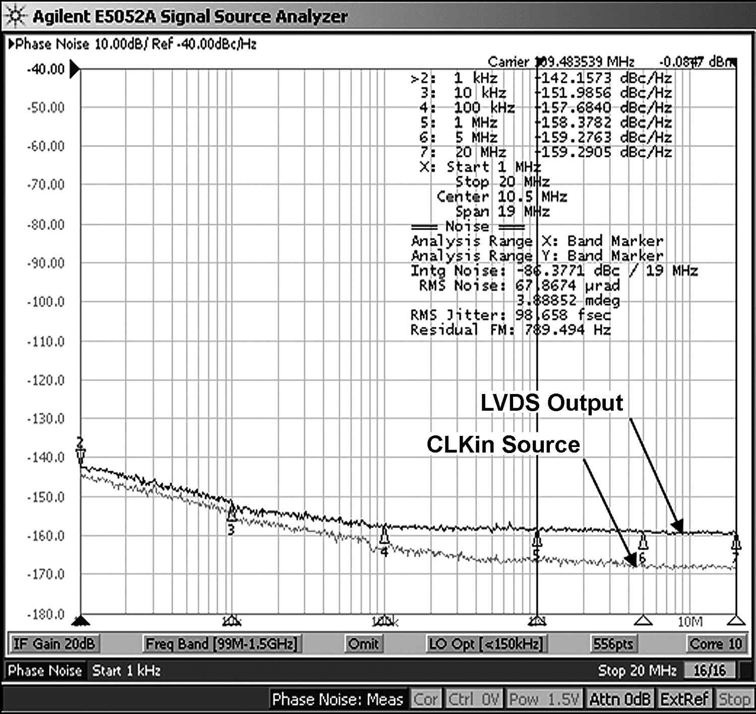
| See Note 1 in Graph Notes table | ||
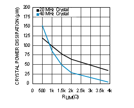
| See Notes 2 and 3 in Graph Notes table | ||
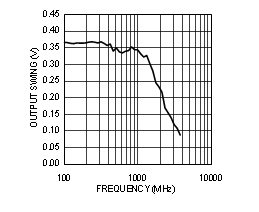
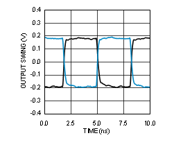
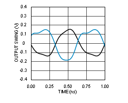
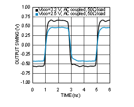
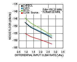
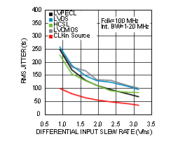
| See Note 1 in Graph Notes | ||
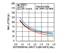
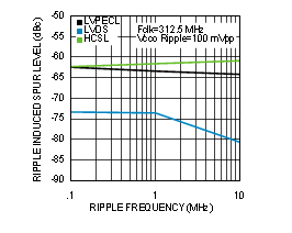
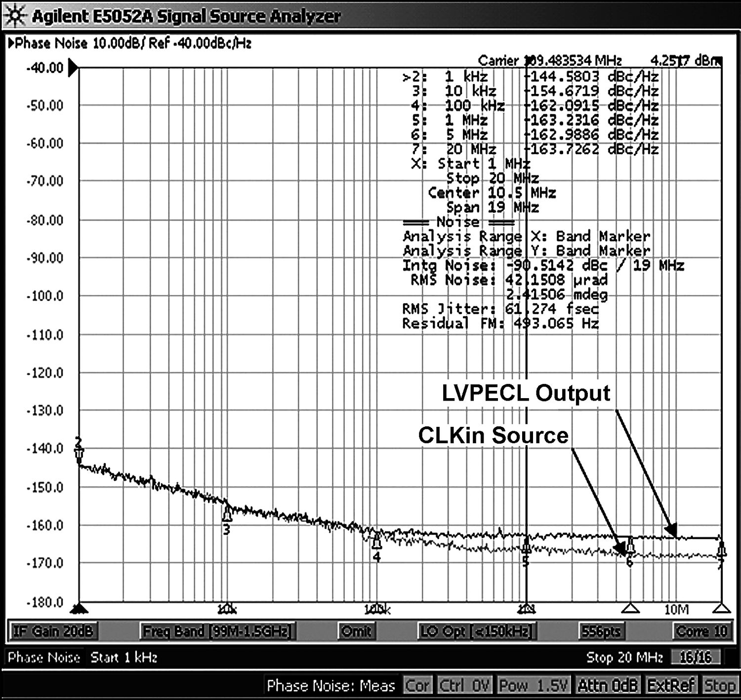
| See Note 1 in Graph Notes table | ||
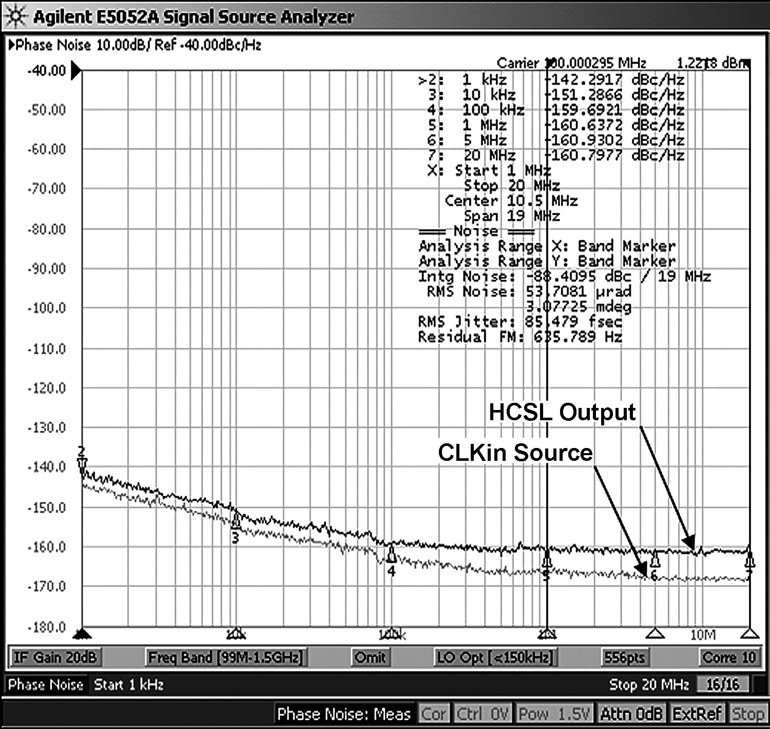
| See Note 1 in Graph Notes table | ||
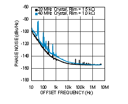
| See Notes 2 and 3 in Graph Notes table. | ||
Table 1. Graph Notes
| NOTE | ||||
|---|---|---|---|---|
| (1) | The typical RMS jitter values in the plots show the total output RMS jitter (JOUT) for each output buffer type and the source clock RMS jitter (JSOURCE). From these values, the Additive RMS Jitter can be calculated as: JADD = SQRT(JOUT2 - JSOURCE2). | |||
| (2) | 20 MHz crystal characteristics: Abracon ABL series, AT cut, CL = 18 pF , C0 = 4.4 pF measured (7 pF max), ESR = 8.5 Ω measured (40 Ω max), and Drive Level = 1 mW max (100 µW typical). | |||
| (3) | 40 MHz crystal characteristics: Abracon ABLS2 series, AT cut, CL = 18 pF , C0 = 5 pF measured (7 pF max), ESR = 5 Ω measured (40 Ω max), and Drive Level = 1 mW max (100 µW typical). | |||