SNAS522K September   2011  – December 2023 LMK03806

PRODUCTION DATA  

  1.   1
  2. Features
  3. Applications
  4. Description
  5. Pin Configuration and Functions
  6. Specifications
    1. 5.1 Absolute Maximum Ratings
    2. 5.2 ESD Ratings
    3. 5.3 Recommended Operating Conditions
    4. 5.4 Thermal Information
    5. 5.5 Electrical Characteristics
    6. 5.6 Timing Requirements
    7. 5.7 Typical Characteristics
  7. Parameter Measurement Information
    1. 6.1 Differential Voltage Measurement Terminology
  8. Detailed Description
    1. 7.1 Overview
    2. 7.2 Functional Block Diagrams
    3. 7.3 Features Description
      1. 7.3.1 Serial MICROWIRE Timing Diagram and Terminology
      2. 7.3.2 Crystal Support With Buffered Outputs
      3. 7.3.3 Integrated Loop Filter Poles
      4. 7.3.4 Integrated VCO
      5. 7.3.5 Clock Distribution
        1. 7.3.5.1 CLKout DIvider
        2. 7.3.5.2 Programmable Output Type
        3. 7.3.5.3 Clock Output Synchronization
      6. 7.3.6 Default Start-Up Clocks
    4. 7.4 Device Functional Modes
    5. 7.5 Programming
      1. 7.5.1 General Information
        1. 7.5.1.1 Special Programming Case for R0 to R5 for CLKoutX_Y_DIV > 25
        2. 7.5.1.2 Recommended Initial Programming Sequence
        3. 7.5.1.3 READBACK
          1. 7.5.1.3.1 Readback Example
  9. Application and Implementation
    1. 8.1 Application Information
      1. 8.1.1 Crystal Interface
      2. 8.1.2 Driving OSCin Pins With a Single-Ended Source
      3. 8.1.3 Driving OSCin Pins With a Differential Source
      4. 8.1.4 Frequency Planning With the LMK03806
      5. 8.1.5 Configuring the PLL
        1. 8.1.5.1 Example PLL Configuration
      6. 8.1.6 Digital Lock Detect
    2. 8.2 Typical Application
      1. 8.2.1 Design Requirements
      2. 8.2.2 Detailed Design Procedure
        1. 8.2.2.1 Device Selection
          1. 8.2.2.1.1 Clock Architect
          2. 8.2.2.1.2 Clock Design Tool
          3. 8.2.2.1.3 Calculation Using LCM
        2. 8.2.2.2 Device Configuration
        3. 8.2.2.3 PLL Loop Filter Design
          1. 8.2.2.3.1 Example Loop Filter Design
        4. 8.2.2.4 Other Device Specific Configuration
          1. 8.2.2.4.1 Digital Lock Detect
        5. 8.2.2.5 Device Programming
      3. 8.2.3 Application Curves
    3. 8.3 System Examples
      1. 8.3.1 System Level Diagram
    4. 8.4 Best Design Practices
      1. 8.4.1 LVCMOS Complementary vs. Non-Complementary Operation
      2. 8.4.2 LVPECL Outputs
      3. 8.4.3 Sharing MICROWIRE (SPI) Lines
      4. 8.4.4 SYNC Pin
      5. 8.4.5 CLKout Vcc Pins
    5. 8.5 Power Supply Recommendations
      1. 8.5.1 Current Consumption and Power Dissipation Calculations
    6. 8.6 Layout
      1. 8.6.1 Layout Guidelines
      2. 8.6.2 Layout Example
  10. Device and Documentation Support
    1. 9.1 Device Support
      1. 9.1.1 Development Support
    2. 9.2 Documentation Support
      1. 9.2.1 Related Documentation
    3. 9.3 Receiving Notification of Documentation Updates
    4. 9.4 Support Resources
    5. 9.5 Trademarks
    6. 9.6 Electrostatic Discharge Caution
    7. 9.7 Glossary
  11. 10Register Maps
    1. 10.1  Default Device Register Settings After Power On Reset
    2. 10.2  Register R0 TO R5
      1. 10.2.1 CLKoutX_Y_PD, Powerdown CLKoutX_Y Output Path
      2. 10.2.2 RESET
      3. 10.2.3 POWERDOWN
      4. 10.2.4 CLKoutX_Y_DIV, Clock Output Divide
    3. 10.3  Registers R6 TO R8
      1. 10.3.1 CLKoutX_TYPE
    4. 10.4  REGISTER R9
    5. 10.5  REGISTER R10
      1. 10.5.1 OSCout1_TYPE, LVPECL Output Amplitude Control
      2. 10.5.2 OSCout0_TYPE
      3. 10.5.3 EN_OSCoutX, OSCout Output Enable
      4. 10.5.4 OSCoutX_MUX, Clock Output Mux
      5. 10.5.5 OSCout_DIV, Oscillator Output Divide
    6. 10.6  REGISTER R11
      1. 10.6.1 NO_SYNC_CLKoutX_Y
      2. 10.6.2 SYNC_POL_INV
      3. 10.6.3 SYNC_TYPE
      4. 10.6.4 EN_PLL_XTAL
    7. 10.7  REGISTER R12
      1. 10.7.1 LD_MUX
      2. 10.7.2 LD_TYPE
      3. 10.7.3 SYNC_PLL_DLD
    8. 10.8  REGISTER R13
      1. 10.8.1 READBACK_TYPE
      2. 10.8.2 GPout0
    9. 10.9  REGISTER 14
      1. 10.9.1 GPout1
    10. 10.10 REGISTER 16
    11. 10.11 REGISTER 24
      1. 10.11.1 PLL_C4_LF, PLL Integrated Loop Filter Component
      2. 10.11.2 PLL_C3_LF, PLL Integrated Loop Filter Component
      3. 10.11.3 PLL_R4_LF, PLL Integrated Loop Filter Component
      4. 10.11.4 PLL_R3_LF, PLL Integrated Loop Filter Component
    12. 10.12 REGISTER 26
      1. 10.12.1 EN_PLL_REF_2X, PLL Reference Frequency Doubler
      2. 10.12.2 PLL_CP_GAIN, PLL Charge Pump Current
      3. 10.12.3 PLL_DLD_CNT
    13. 10.13 REGISTER 28
      1. 10.13.1 PLL_R, PLL R Divider
    14. 10.14 REGISTER 29
      1. 10.14.1 OSCin_FREQ, PLL Oscillator Input Frequency Register
      2. 10.14.2 PLL_N_CAL, PLL N Calibration Divider
    15. 10.15 REGISTER 30
      1. 10.15.1 PLL_P, PLL N Prescaler Divider
      2. 10.15.2 PLL_N, PLL N Divider
    16. 10.16 REGISTER 31
      1. 10.16.1 READBACK_ADDR
      2. 10.16.2 uWire_LOCK
  12. 11Revision History
  13. 12Mechanical, Packaging, and Orderable Information

Package Options

Mechanical Data (Package|Pins)
Thermal pad, mechanical data (Package|Pins)
Orderable Information

Default Start-Up Clocks

Before the LMK03806 is programmed some clocks will operate at default frequencies upon power up. The active output clocks depend upon the reference input type. If a crystal reference is used with OSCin, only CLKout8 will operate at a nominal VCO frequency /25. When an XO or other external reference is used as a reference with OSCin, OSCout0 will buffer the OSCin frequency in addition to CLKout8 operating at a nominal VCO frequency /25. These clocks can be used to clock external devices such as microcontrollers, FPGAs, CPLDs, and so forth, before the LMK03806 is programmed. Refer to Figure 7-5 or Figure 7-6 for illustration of start-up clocks.

The nominal VCO frequency of CLKout8 on power up will typically be 98 MHz.

Note during programming CLKout8 may momentarily stop or glitch during the VCO calibration routine.
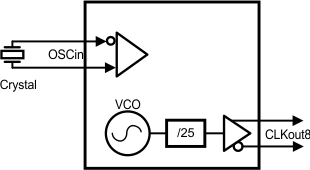
GUID-A07CFB62-24D1-45FA-A96A-B5186AC39681-low.gifFigure 7-5 Start-Up Clock Using Crystal Reference
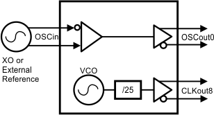
GUID-ECFD1E36-0F04-44BB-ADBC-5AB61BF57BE6-low.gifFigure 7-6 Start-Up Clock Using XO or Other External Reference