SNAS676D October 2015 – October 2017 LMK61A2-100M , LMK61A2-125M , LMK61A2-156M , LMK61A2-312M , LMK61A2-644M , LMK61E0-050M , LMK61E0-155M , LMK61E0-156M , LMK61E2-100M , LMK61E2-125M , LMK61E2-156M , LMK61E2-312M , LMK61I2-100M
PRODUCTION DATA.
- 1 Features
- 2 Applications
- 3 Description
- 4 Revision History
- 5 Pin Configuration and Functions
-
6 Specifications
- 6.1 Absolute Maximum Ratings
- 6.2 ESD Ratings
- 6.3 Recommended Operating Conditions
- 6.4 Thermal Information
- 6.5 Electrical Characteristics - Power Supply
- 6.6 LVPECL Output Characteristics
- 6.7 LVDS Output Characteristics
- 6.8 HCSL Output Characteristics
- 6.9 OE Input Characteristics
- 6.10 Frequency Tolerance Characteristics
- 6.11 Power-On/Reset Characteristics (VDD)
- 6.12 PSRR Characteristics
- 6.13 PLL Clock Output Jitter Characteristics
- 6.14 Typical 156.25-MHz Output Phase Noise Characteristics
- 6.15 Additional Reliability and Qualification
- 6.16 Typical Characteristics
- 7 Parameter Measurement Information
- 8 Power Supply Recommendations
- 9 Layout
- 10Device and Documentation Support
- 11Mechanical, Packaging, and Orderable Information
Package Options
Refer to the PDF data sheet for device specific package drawings
Mechanical Data (Package|Pins)
- SIA|6
Thermal pad, mechanical data (Package|Pins)
Orderable Information
7 Parameter Measurement Information
7.1 Device Output Configurations
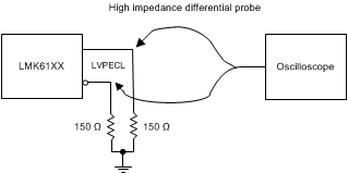
 Figure 10. LVPECL Output DC Configuration During Device Test
 Figure 11. LVDS Output DC Configuration During Device Test
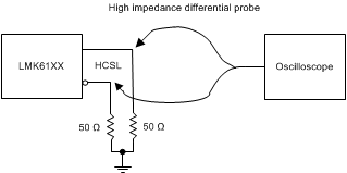
 Figure 12. HCSL Output DC Configuration During Device Test
 Figure 13. LVPECL Output AC Configuration During Device Test
 Figure 14. LVDS Output AC Configuration During Device Test
 Figure 15. HCSL Output AC Configuration During Device Test
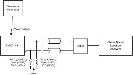
 Figure 16. PSRR Test Setup
 Figure 17. Differential Output Voltage and Rise/Fall Time