SNOSAR2H September 2008 – April 2016 LMP8601 , LMP8601-Q1 , LMP8602 , LMP8602-Q1 , LMP8603 , LMP8603-Q1
PRODUCTION DATA.
- 1 Features
- 2 Applications
- 3 Description
- 4 Revision History
- 5 Pin Configuration and Functions
- 6 Specifications
- 7 Detailed Description
- 8 Application and Implementation
- 9 Power Supply Recommendations
- 10Layout
- 11Device and Documentation Support
- 12Mechanical, Packaging, and Orderable Information
Package Options
Mechanical Data (Package|Pins)
Thermal pad, mechanical data (Package|Pins)
Orderable Information
7 Detailed Description
7.1 Overview
The LMP860x and LMP860x-Q1 are fixed gain differential voltage precision amplifiers, with a –22-V to +60-V input common-mode voltage range when operating from a single 5-V supply, or a –4-V to +27-V input common-mode voltage range when operating from a single 3.3-V supply. The LMP8601 and LMP8601-Q1 have a gain of 20x, the LMP8602 and LMP8602-Q1 have a gain of 50x, and the LMP8603 and LMP8603-Q1 have a gain of 100x.
The LMP860x and LMP860x-Q1 are members of the LMP family and are ideal parts for unidirectional and bidirectional current sensing applications. Because of the proprietary chopping level-shift input stage, the LMP860x and LMP860x-Q1 achieve very low offset, very low thermal offset drift, and very high CMRR. The LMP860x and LMP860x-Q1 amplify and filter small differential signals in the presence of high common-mode voltages.
The LMP860x and LMP860x-Q1 use level shift resistors at the inputs. Because of these resistors, the LMP860x and LMP860x-Q1 can easily withstand very large differential input voltages that may exist in fault conditions where some other less protected high-performance current sense amplifiers might sustain permanent damage.
7.1.1 Theory of Operation
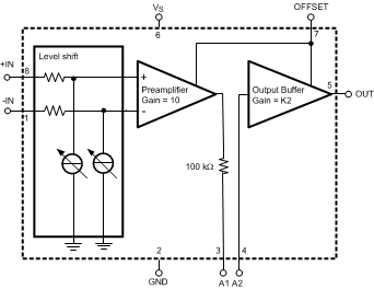
The schematic shown in the Functional Block Diagram gives a basic representation of the internal operation of the LMP860x and LMP860x-Q1.
The signal on the input pins is typically a small differential voltage developed across a current sensing shunt resistor. The input signal may also appear at a high common-mode voltage. The input signals are accessed through two input resistors that change the voltage into a current. The proprietary chopping level-shift current circuit pulls or pushes current through the input resistors to bring the common-mode voltage behind these resistors within the supply rails.
Subsequently, the signal is gained up by a factor of 10 and brought out on the A1 pin through a trimmed 100-kΩ resistor. In the application, additional gain adjustment or filtering components can be added between the A1 and A2 pins as explained in subsequent sections. The signal on the A2 pin is further amplified by a factor of 2 (LMP8601 and LMP8601-Q1), 5 (LMP8602, LMP8602-Q1), or 10 (LMP8603, LMP8603-Q1), and brought out on the OUT pin.
7.2 Functional Block Diagram
7.3 Feature Description
7.3.1 Offset Input Pin
The OFFSET pin allows the output signal to be level-shifted to enable bidirectional current sensing. The output signal is bidirectional and mid-rail referenced when the offset pin is connected to the positive supply rail. With the offset pin connected to ground, the output signal is unidirectional and ground-referenced.
The signal on the A1 and OUT pins is ground-referenced when the offset pin is connected to ground. This means that the output signal can only represent positive values of the current through the shunt resistor, so only currents flowing in one direction can be measured.
When the offset pin is tied to the positive supply rail, the signal on the A1 and OUT pins is referenced to a mid-rail voltage which allows bidirectional current sensing. The operation of the amplifier will be fully bidirectional and symmetrical around 0 V differential at the input pins. The signal at the output will follow this voltage difference multiplied by the gain and at an offset voltage at the output of half VS.
When the offset pin is connected to an external voltage source, the output signal will be level shifted to that voltage divided by two. In principle, the output signal can be shifted to any voltage between 0 and VS / 2 by applying twice that voltage to the OFFSET pin.
NOTE
The OFFSET pin must be driven from a very low-impedance source (< 10 Ω). This low source impedance is required because the OFFSET pin internally connects directly to the resistive feedback networks of the two gain stages. When the OFFSET pin is driven from a relatively large impedance (for example, a resistive divider between the supply rails), accuracy decreases.
Examples:
- LMP8601, LMP8601-Q1: A 5-V supply, a gain of 20x, OFFSET pin tied to VS, and a differential input signal of 10 mV results in 2.7 V at the output pin. Similarly, –10 mV at the input results in 2.3 V at the output pin.
- LMP8602, LMP8602-Q1: A 5-V supply, a gain of 50x, and a differential input signal of 10 mV results in 3.0 V at the output pin. Similarly, –10 mV at the input results in 2.0 V at the output pin.
- LMP8603, LMP8603-Q1: A 5-V supply, a gain of 100x, and a differential input signal of 10 mV results in 3.5 V at the output pin. Similarly, –10 mV at the input results in 1.5 V at the output pin.
7.3.2 Additional Second-Order Low-Pass Filter
The LMP86x1 and LMP86x1-Q1 have a third-order Butterworth lowpass characteristic with a typical bandwidth of 60 kHz integrated in the preamplifier stage. The bandwidth of the output buffer can be reduced by adding a capacitor on the A1 pin to create a first-order low-pass filter with a time constant determined by the 100-kΩ internal resistor and the external filter capacitor.
It is also possible to create an additional second-order, Sallen-Key, low-pass filter by adding external components R2, C1 and C2. Together with the internal 100-kΩ resistor R1 as illustrated in Figure 53, this circuit creates a second-order, low-pass filter characteristic.
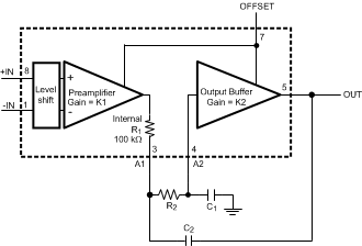
When the corner frequency of the additional filter is much lower than 60 kHz, the transfer function of the described amplifier can be written as:

where
- K1 equals the gain of the preamplifier and K2 that of the buffer amplifier.
Equation 1 can be written in the normalized frequency response for a second-order lowpass filter:

The cutoff frequency ωo in rad/sec (divide by 2π to get the cut-off frequency in Hz) is given by:

and the quality factor of the filter is given by:

With K2 = 2x, Equation 4 transforms results in:

For any filter gain K > 1x, the design procedure can be very simple if the two capacitors are chosen to in a certain ratio.

Inserting this in Equation 4 for Q results in:

Which results in:

In this case, given the predetermined value of R1 = 100 kΩ (the internal resistor), the quality factor is set solely by the value of the resistor R2.
R2 can be calculated based on the desired value of Q as the first step of the design procedure with the following equation:

For the gain of 2 for the LMP8601 and LMP8601-Q1, the result is:

For the gain of 5 for the LMP8602 and LMP8602-Q1, the result is:

For the gain of 10 for the LMP8603 and LMP8603-Q1, the result is:

For instance, the value of Q can be set to 0.5√2 to create a Butterworth response, to 1/√3 to create a Bessel response, or a 0.5 to create a critically damped response. After the value of R2 has been found, the second and last step of the design procedure is to calculate the required value of C to give the desired low-pass cut-off frequency using:

For the gain = 2, the result is:

The gain = 5 results in:

The gain = 10 gives:

For C2 the value is calculated with:

For a gain = 2:
Or for a gain = 5:

And for a gain = 10:

Note that the frequency response achieved using this procedure is only accurate if the cut-off frequency of the second-order filter is much smaller than the intrinsic 60-kHz, low-pass filter. In other words, choose the frequency response of the LMP860x or LMP860x-Q1 circuit so that the internal poles do not affect the external second-order filter.
7.4 Device Functional Modes
7.4.1 Gain Adjustment
The gain of the LMP860x and LMP860x-Q1 is fixed; however, the overall gain may be adjusted as the signal path between the two internal amplifiers is available on the A1 and A2 pins.
7.4.1.1 Reducing Gain
Figure 54 shows the configuration that can be used to reduce the gain of the LMP8601 and LMP8601-Q1.
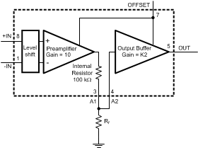
Rr creates a resistive divider together with the internal 100-kΩ resistor such that the reduced gain Gr becomes:

For the LMP8602 and LMP8602-Q1:

And for the LMP8603 and LMP8603-Q1:

Given a desired value of the reduced gain Gr, using this equation, the LMP8601 and LMP8601-Q1 required value for the Rr is calculated with:

For the LMP8602 and LMP8602-Q1:

And for the LMP8603 and LMP8603-Q1:

7.4.1.2 Increasing Gain
Figure 55 shows the configuration that can be used to increase the gain of the LMP8601 and LMP8601-Q1.
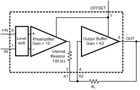
Ri creates positive feedback from the output pin to the input of the buffer amplifier. The positive feedback increases the gain. The increased gain Gi for the LMP8601 and LMP8601-Q1 becomes:

For the LMP8602 and LMP8602-Q1:

And for the LMP8603 and LMP8603-Q1:

From this equation, for a desired value of the gain, the LMP8601 and LMP8601-Q1 required value of Ri is calculated with:

For the LMP8602 and LMP8602-Q1:

And for the LMP8603 with:

Note that from the equation for the gain Gi, for large gains, Ri approaches 100 kΩ. In this case, the denominator in the equation becomes close to zero. In practice, for large gains, the denominator is determined by tolerances in the value of the external resistor Ri and the internal 100-kΩ resistor. In this case, the gain becomes very inaccurate. If the denominator becomes equal to zero, the system becomes unstable. TI recommends to limit the application of this technique to gain values of 50 or smaller.
7.4.2 Driving Switched Capacitive Loads
Some ADCs load their signal source with a sample and hold capacitor. The capacitor may be discharged prior to being connected to the signal source. If the LMP860x and LMP860x-Q1 are driving such ADCs, the sudden current that should be delivered when the sampling occurs may disturb the output signal. This effect was simulated with the circuit shown in Figure 56 where the output is to a capacitor that is driven by a rail-to-rail square wave.
 Figure 56. Driving Switched Capacitive Load
This circuit simulates the switched connection of a discharged capacitor to the LMP860x and LMP860x-Q1 output. The resulting VOUT disturbance signals are shown in Figure 57 and Figure 58.
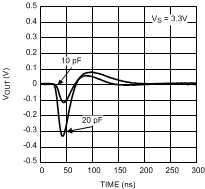 Figure 57. Capacitive Load Response at 3.3 V
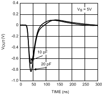 Figure 58. Capacitive Load Response at 5.0 V
These figures can be used to estimate the disturbance that will be caused when driving a switched capacitive load. To minimize the error signal introduced by the sampling that occurs on the ADC input, place an additional RC filter between the LMP860x or LMP860x-Q1 and the ADC, as illustrated in Figure 59.
 Figure 59. Reduce Error When Driving ADCs
The external capacitor absorbs the charge that flows when the ADC sampling capacitor is connected. The external capacitor should be much larger than the sample-and-hold capacitor at the input of the ADC, and the RC time constant of the external filter should be such that the speed of the system is not affected.