SNOSB29H November   2009  – May 2022 LMP8645 , LMP8645HV

PRODUCTION DATA  

  1. Features
  2. Applications
  3. Description
  4. Revision History
  5. Pin Configuration and Functions
  6. Specifications
    1. 6.1 Absolute Maximum Ratings
    2. 6.2 ESD Ratings
    3. 6.3 Recommended Operating Conditions
    4. 6.4 Thermal Information
    5. 6.5 2.7-V Electrical Characteristics
    6. 6.6 5-V Electrical Characteristics
    7. 6.7 12-V Electrical Characteristics
    8. 6.8 Typical Characteristics
  7. Detailed Description
    1. 7.1 Overview
      1. 7.1.1 Theory of Operation
    2. 7.2 Functional Block Diagram
    3. 7.3 Feature Description
      1. 7.3.1 Driving ADC
      2. 7.3.2 Applying Input Voltage With No Supply Voltage
    4. 7.4 Device Functional Modes
      1. 7.4.1 Selection of the Gain Resistor
      2. 7.4.2 Gain Range Limitations
        1. 7.4.2.1 Range 1: VCM is –2 V to 1.8 V
        2. 7.4.2.2 Range 2: VCM is 1.8 V to VS
        3. 7.4.2.3 Range 3: VCM is greater than VS
      3. 7.4.3 Selection of Sense Resistor
        1. 7.4.3.1 Resistor Power Rating and Thermal Issues
        2. 7.4.3.2 Using PCB Trace as a Sense Resistor
      4. 7.4.4 Sense Line Inputs
        1. 7.4.4.1 Effects of Series Resistance on Sense Lines
  8. Application and Implementation
    1. 8.1 Application Information
    2. 8.2 Typical Applications
      1. 8.2.1 Typical Current Monitor Application
        1. 8.2.1.1 Design Requirements
        2. 8.2.1.2 Detailed Design Procedure
        3. 8.2.1.3 Application Curves
      2. 8.2.2 High Brightness LED Driver
  9. Power Supply Recommendations
  10. 10Layout
    1. 10.1 Layout Guidelines
    2. 10.2 Layout Example
  11. 11Device and Documentation Support
    1. 11.1 Device Support
      1. 11.1.1 Development Support
    2. 11.2 Documentation Support
      1. 11.2.1 Related Documentation
    3. 11.3 Receiving Notification of Documentation Updates
    4. 11.4 Support Resources
    5. 11.5 Trademarks
    6. 11.6 Electrostatic Discharge Caution
    7. 11.7 Glossary
  12. 12Mechanical, Packaging, and Orderable Information

Package Options

Mechanical Data (Package|Pins)
Thermal pad, mechanical data (Package|Pins)
Orderable Information

Range 2: VCM is 1.8 V to VS

In this range, the maximum voltage at the RG pin is related to the common-mode voltage and VSENSE. So all the RGAIN resistor values which respect the following inequalities are allowed:

Equation 5. VRG ≤ min (Vout_max; (VCM – Vsense– 250 mV))

where

The graphical representation in Figure 7-4 helps in the selection.

All the combinations (VSENSE, RGAIN) below the curves for given VCM and supply voltage are allowed.
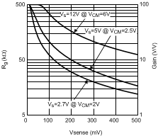
GUID-F6A9CC08-F749-45B3-987D-AE8D23E8D507-low.gifFigure 7-4 Allowed Gains for Range 2

Also in this range, once selected, the RGAIN (Gain) and the VSENSE range is fixed too.