SNAS634B March 2014 – January 2016 LMP92066
PRODUCTION DATA.
- 1 Features
- 2 Applications
- 3 Description
- 4 Simplified Schematic
- 5 Revision History
- 6 Pin Configuration and Functions
- 7 Specifications
-
8 Detailed Description
- 8.1 Overview
- 8.2 Functional Block Diagram
- 8.3 Features Description
- 8.4 Device Functional Modes
- 8.5
Programming
- 8.5.1 Temperature Sensor Output Data Access Registers
- 8.5.2 DAC Input Data Registers
- 8.5.3 Temperature Sensor Status Register
- 8.5.4 Override Control Register
- 8.5.5 Override Data Registers
- 8.5.6 EEPROM Control Register
- 8.5.7 Software RESET Register
- 8.5.8 Access Control Register
- 8.5.9 Block I2C Access Control Register
- 8.5.10 I2C Address LOCK Register
- 8.5.11 Output Drive Supply Status Register
- 8.5.12 Device Version Register
- 8.5.13 EEPROM Burn Counter
- 8.5.14 LUT Coefficient Registers
- 8.5.15 LUT Control Registers
- 8.5.16 Notepad Registers
- 8.6 Register Map
- 9 Application and Implementation
- 10Power Supply Recommendations
- 11Layout
- 12Device and Documentation Support
- 13Mechanical, Packaging, and Orderable Information
Package Options
Mechanical Data (Package|Pins)
- PWP|16
Thermal pad, mechanical data (Package|Pins)
- PWP|16
Orderable Information
9 Application and Implementation
NOTE
Information in the following applications sections is not part of the TI component specification, and TI does not warrant its accuracy or completeness. TI’s customers are responsible for determining suitability of components for their purposes. Customers should validate and test their design implementation to confirm system functionality.
9.1 Application Information
The LMP92066 was designed for ease of use. The device requires minimum external components to realize its full functionality. In the typical application the bulk of the design effort is spent on characterization of the target transfer function, and then developing a set of coefficients that the LMP92066 to accurately reproduce the target function.
NOTE
The LMP92066 can approximate temperature dependent functions, VDAC0,1(T), only if the following requirements are met:
- Each VDAC0,1(T) must be unipolar. The range of the function must be either wholly positive, or wholly negative. This is dictated by the structure of the Buffer Amplifier that drives the FETDRVx. See the Buffer Amplifier section.
- Both functions VDAC0,1(T) must be of the same polarity. See the Buffer Amplifier section.
- Each VDAC0,1(T) must be monotonic. This is dictated by the structure of the LUTs. See the LUT and ALU Organization section.
- The maximum slope of each VDAC0,1(T) is no greater than 4.88 mV/°C. This also limits the maximum range, the minimum to maximum span, for the VDAC0,1(T) to 761 mV. This is due to the fact that the LUT stores the slope of the VDAC0,1(T) as 4-bit values. See the The LUT Input and Output Ranges section.
9.2 Typical Applications
9.2.1 Temperature Compensated Bias Generator for LDMOS Power Amplifer (PA)
The typical application for the LMP92066 is the biasing of the power amplifiers in an RF system. What is required in such applications is for the PA drain current to remain constant over a wide range of operating temperatures. The LMP92066 senses the PA temperature and adjust the bias potential at the gate of the PA in accordance with the known VGS(T), at ID = constant, characteristic of the PA.
The typical application circuit for LDMOS applications is shown in Figure 39. A thermal path has to be provided between the LMP92066 and the PA. This is typically accomplished through the close proximity of the 2 devices, and the common metal layer. See also the Layout Example.
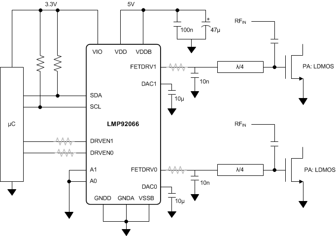 Figure 39. Temperature-Compensated Bias Generator
for LDMOS Power Amplifier (PA)
9.2.1.1 Design Requirements
The thermal characteristic of a hypothetical LDMOS PA is plotted in Figure 40. This characteristic was obtained from the temperature sweep of the LDMOS gate-source voltage, VGS, while keeping the drain current, ID = 750 mA. The goal is to have the LMP92066 produce that same VGS vs T characteristic which, when applied to the gate of the PA device ensures constant ID throughout the operating temperature range.
In the following sections the curve VGS vs T are referred to as the Target Function, VDAC (T).
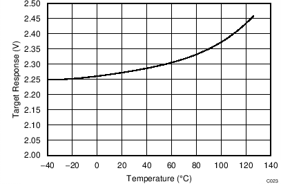 Figure 40. Target Function to be Reproduced by the LMP92066:
VGS vs T Characteristic of an LDMOS PA
The target function is approximated by the following polynomial (T unit is °C):

In the Detailed Design Requirements section the above expression is used to obtain the LUT coefficient values.
9.2.1.2 Detailed Design Requirements
Figure 41 outlines the LUT design procedure. The procedure is for one channel only – repeat for the second available channel, as needed. In principle, the procedure follows the signal path backwards from the output, which is ideally the target function VDAC(T), back to the LUT coefficients, and each block’s processing has to be “reversed”. Additional comments for each design step are listed below Figure 41.
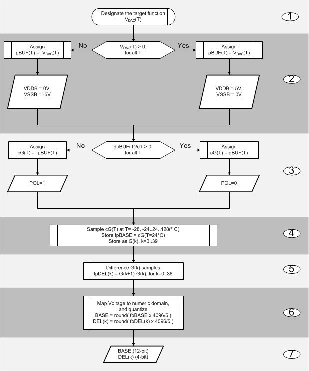 Figure 41. Flowchart of the Generalized LUT Design Procedure
- Before attempting to calculate the LUT coefficients for the given target function VDAC(T), verify the requirements listed in the Application Information section are met.
- Test if the function is wholly positive, or negative. If necessary “undo” the action of the Buffer Amplifier. (See the Buffer Amplifier section.) From now on consider the pre-buffer signal pBUFF(T). The design variable set in this step is the state of the VDDB and VSSB supplies. VDAC(T) is a strictly positive valued function, therefore:
- Check the slope of the pBUF(T). Record the sign of the slope, and from here on consider a positive slope function cG(T). The design variable set in this step is the POL bit. pBUFF(T) is a monotonically increasing function, therefore:
- Discretize the continuous cG(T) along its temperature domain, thus creating the sequence G(k). Maintain the full precision of the G(k) values. Note the full precision cG(T) at T = 24°C — this is the full precision BASE value, fpBASE, still in voltage domain.
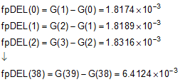
- Apply difference operation to the G(k) sequence, and obtain new sequence fpDEL(k). These are now the full precision increments of the target function with each 4°C interval.
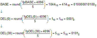
- Convert the full precision voltages of fpDEL(k) and fpBASE to a numeric, quantized domain. This reverses the DAC action.
- Usually BYP bit is reset, BYP=0. However, in cases where it is desirable to bypass the LUT and ALU, and have the DACx output produce voltage equivalent of the BASE value, set BYP = 1.
- Repeat steps 1 to 6 to obtain POL, BYP, BASE, DELx values for the second channel.
- Now have BYP, POL, BASE, and DEL(0..38) values ready to be programmed into the LUT.


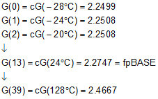
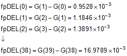
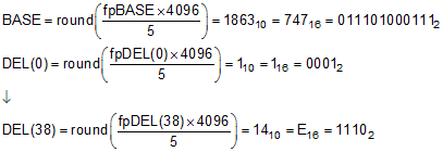
NOTE
The device has to be in the L2 Access Level before commencing the WRITE access of BYP, POL, BASE, DELx values. The register WRITE operation immediately affects the operation of the device. However, operating memory is volatile, and BURN operation is required to commit the LUT coefficients to non-volatile memory, EEPROM.
9.2.1.3 Application Curves
The output of the LMP92066 due to the coefficients calculated in the above procedure is shown in Figure 42.
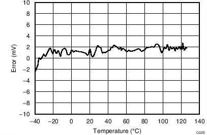
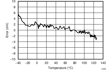
Figure 43 shows the absolute difference between the target function and the measured response of the LMP92066.
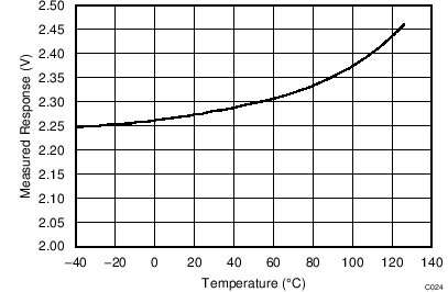 Figure 42. Measured Response of the LMP92066
Resulting from the LUT Coefficients
(see Detailed Design Requirements)
9.2.2 Temperature Compensated Bias Generator for GaN Power Amplifer (PA)
The typical application for the LMP92066 is the biasing of the power amplifiers in an RF system. What is required in such applications is for the PA drain current to stay constant over a wide range of operating temperatures. The LMP92066 senses the PA temperature and adjust the bias potential at the gate of PA in accordance with the known VGS(T), at ID = constant, characteristic of the PA.
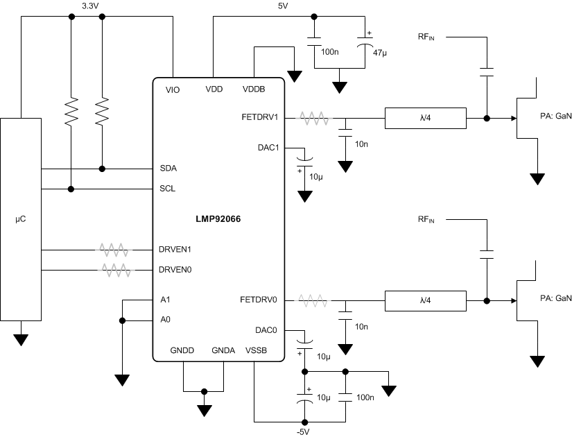 Figure 44. Temperature-Compensated Bias Generator
for GaN Power Amplifier (PA)
9.2.2.1 Design Requirements
The thermal characteristic of a hypothetical GaN PA is plotted in Figure 45. This characteristic was obtained from the temperature sweep of the GaN gate-source voltage, VGS, while keeping the drain current, ID = 750 mA. The goal is to have the LMP92066 produce that same VGS vs T characteristic which, when applied to the gate of the PA device ensures constant ID throughout the operating temperature range.
In the following sections the curve VGS vs T is referred to as the Target Function, VDAC (T).
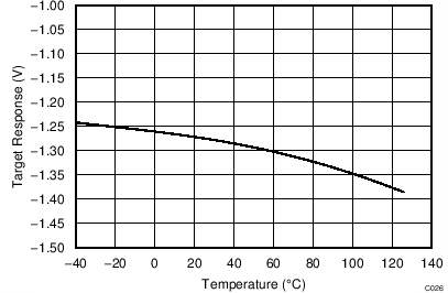 Figure 45. The Target Function to be Reproduced by the LMP92066:
 VGS vs T Characteristic of an GaN PA
The target function is approximated by the following polynomial (T unit is °C):
9.2.2.2 Detailed Design Procedure
Figure 46 outlines the LUT design procedure. The procedure is for one channel only – repeat for the second available channel, as needed.
In principle, the procedure follows the signal path backwards from the output, which is ideally the target function VDAC(T), back to the LUT coefficients, reversing the processing of each block. Additional comments for each design step are listed below Figure 46.
 Figure 46. Flowchart of the Generalized LUT Design Procedure
- Before attempting to calculate the LUT coefficients for the given target function VDAC(T), verify the requirements listed in the Application Information section are met.
- Test if the function is wholly positive, or negative. If necessary “undo” the action of the Buffer Amplifier. (See the Buffer Amplifier section.) From now on consider the pre-buffer signal pBUFF(T). The design variable set in this step is the state of the VDDB, VSSB supplies. VDAC(T) is a strictly positive valued function, therefore:
- Check the slope of the pBUF(T). Record the sign of the slope, and from here on consider a positive slope function cG(T). The design variable set in this step is the POL bit. pBUFF(T) is a monotonically increasing function, therefore:
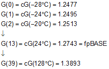
- Discretize the continuous cG(T) along its temperature domain, thus creating the sequence G(k). Maintain the full precision of the G(k) values. Note the full precision cG(T) at T = 24°C — this is the full precision BASE value, fpBASE, still in voltage domain.
- Apply difference operation to the G(k) sequence, and obtain new sequence fpDEL(k). These are now the full precision increments of the target function with each 4°C interval.
- Convert the full precision voltages of fpDEL(k) and fpBASE to a numeric, quantized domain. This reverses the DAC action.
- Usually BYP bit is reset, BYP=0. However, in cases where it is desirable to bypass the LUT and ALU, and have the DACx output produce voltage equivalent of the BASE value, set BYP = 1.
- Repeat steps 1 to 6 to obtain POL, BYP, BASE, DELx values for the second channel.
- Now have BYP, POL, BASE, and DEL(0..38) values ready to be programmed into the LUT.


NOTE
The device has to be in the L2 Access Level before commencing the WRITE access of BYP, POL, BASE, DELx values. The register WRITE operation immediately affects the operation of the device. However, operating memory is volatile, and BURN operation is required to commit the LUT coefficients to non-volatile memory, EEPROM.
9.2.2.3 Application Curves
The output of the LMP92066 due to the coefficients calculated in the above procedure is shown in Figure 47.
Figure 48 shows the absolute difference between the target function and the measured response of the LMP92066.
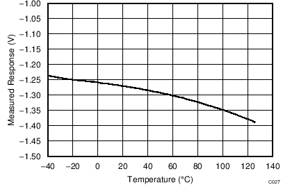 Figure 47. Measured Response of the LMP92066 Resulting from the LUT Coefficients
(see Detailed Design Procedure)
9.3 Do's and Don'ts
9.3.1 Output Drive Switching
Some applications may require that the FETDRVx output reaches the level set by the DACx as fast as possible after the assertion of DRVENx.
There are parameters which determine the delay between the assertion of DRVENx, and the FETDRVx output achieving its final level as set by the DACx:
- The delay between the DRVENx input the output switch.
- The charge up time of the FETDRVx node once the output switch is closed.
The delay of the switch response to the DRVENx input, tON, is specified in the Electrical Characteristics table.
The charge up time of the FETDRVx node is dependent on the selection of the external components. Rapid rise time of the FETDRVx output, is made possible through the use of the external capacitor C1. C1 is always charged to the potential generated by the DACx, and used to provide instantaneous charge to the load present at the FETDRVx when the output switch closes – the switch between DACx and FETDRVx pin.
C1 is chosen to be several orders of magnitude larger than the total capacitance present at the FETDRVx pin, CEXT. In the typical application C1 is 10 µF, and CEXT is limited to 10 nF. See Figure 49. When the output switch closes, a current flows from the C1, acting as a reservoir, to CEXT. This charge-up current is limited only by the resistance of the output switch RDRV, resulting in very rapid slewing at the FETDRVx pin. RDRV is specified in the Electrical Characteristics table.
For example, given the following parameters.
- tON = 50 ns
- RDRV = 5 Ω
- CEXT = 10 nF
The total delay time between activation of DRVENx and FETDRVx achieving 95% of its final value is:
NOTE
The charge current flowing into the CEXT at the instant the output switch closes is relatively large and of very short duration, which makes the parasitic inductance in the charge path significant. This parasitic inductance is due to the bond wire and package pin between the device die and the CEXT, and is shown as LP in Figure 49. In some applications it may be beneficial to insert a small resistance in the charge path, see REXT in Figure 49, to dampen the resonance of the LP and CEXT. Choice of REXT is highly application dependent, but 5 Ω is a good initial selection.
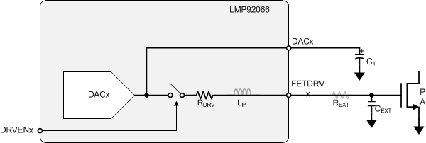 Figure 49. Flow of Charge Current
9.4 Initialization Setup
9.4.1 Factory Default
At the factory the EEPROM is initialized such that all LUT increment values (Δ) are set to 0, BASE value is set to 0x00, and BYP and POL bits are set to 0. This results in the device producing constant output of 0V at DACx pins upon power up, regardless of the temperature or mode or state at the DRVENx inputs.
9.4.2 At Power Up
The device is capable of autonomous operation upon power up, without intervention form the system controller. When the power is applied and reaches the minimum level (approximately 4.1 V) the temperature sensor begins operating, and the internal sequencer begins the transfer of LUT values from the EEPROM to the operating memory. Once the transfer is complete, and the Temperature Sensor has completed the first conversion, the ALU computes the DACs input values, and the DACs start producing output voltages representative of the transfer functions implemented in the LUTs.
The control signal applied to the DRVENx input determines whether the DAC output voltage is present at the FETDRVx output, or that output is driven to VSSB potential.
Figure 50 shows the typical power-up transient behavior at the DACx outputs. While VDD voltage is ramping up from 0 to 5 V the DACx outputs initially follow the VDD. This is due to the fact that initially the device is in the undefined state. When VDD reaches 4.1 V the internal reset occurs and clears the internal data path, resulting in VDACx = 0 V. The Temperature Sensor begins operation at the moment of reset, and 25 ms later produces its first temperature measurement. This, in turn, causes the ALU to update DAC input data, resulting in new VDACx output.
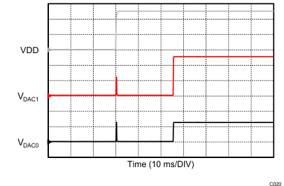
| VDD = 2V/div | VDAC1 = 1V/div | VDAC0 = 1V/div |
See also the Default Operating Mode section.
