SNAS634B March 2014 – January 2016 LMP92066
PRODUCTION DATA.
- 1 Features
- 2 Applications
- 3 Description
- 4 Simplified Schematic
- 5 Revision History
- 6 Pin Configuration and Functions
- 7 Specifications
-
8 Detailed Description
- 8.1 Overview
- 8.2 Functional Block Diagram
- 8.3 Features Description
- 8.4 Device Functional Modes
- 8.5
Programming
- 8.5.1 Temperature Sensor Output Data Access Registers
- 8.5.2 DAC Input Data Registers
- 8.5.3 Temperature Sensor Status Register
- 8.5.4 Override Control Register
- 8.5.5 Override Data Registers
- 8.5.6 EEPROM Control Register
- 8.5.7 Software RESET Register
- 8.5.8 Access Control Register
- 8.5.9 Block I2C Access Control Register
- 8.5.10 I2C Address LOCK Register
- 8.5.11 Output Drive Supply Status Register
- 8.5.12 Device Version Register
- 8.5.13 EEPROM Burn Counter
- 8.5.14 LUT Coefficient Registers
- 8.5.15 LUT Control Registers
- 8.5.16 Notepad Registers
- 8.6 Register Map
- 9 Application and Implementation
- 10Power Supply Recommendations
- 11Layout
- 12Device and Documentation Support
- 13Mechanical, Packaging, and Orderable Information
Package Options
Mechanical Data (Package|Pins)
- PWP|16
Thermal pad, mechanical data (Package|Pins)
- PWP|16
Orderable Information
12 Device and Documentation Support
12.1 Device Support
12.1.1 Device Nomenclature
-
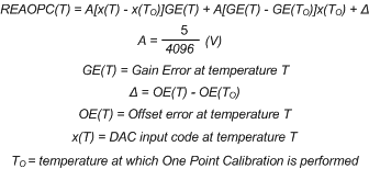
REAOPC
Residual Error After One Point Calibration is the error acquired in the Analog Signal Path due to the inaccuracies of the constituent signal processing blocks: DAC, Buffer Amplifier, internal Reference. REAOPC is dominated by the Offset and Gain temperature drifts, since the significant portion of the initial error is eliminated through the One Point Calibration process. The small contribution from the DAC linearity error (INL) is omitted, since it is numerically insignificant. REAOPC can be predicted through the following formulation:

-
One Point Calibration
One Point Calibration is the process where the output of the LMP92066 is adjusted in the target system to achieve the desired response, at temperature T0. Typically this involves measurement of the overall system output variable; for example, ID of the PA, and modification of the BASE value in the LUT to achieve the desired PA bias current.
12.2 Trademarks
PowerPAD is a trademark of Texas Instruments Incorporated.
All other trademarks are the property of their respective owners.
12.3 Electrostatic Discharge Caution

These devices have limited built-in ESD protection. The leads should be shorted together or the device placed in conductive foam during storage or handling to prevent electrostatic damage to the MOS gates.
12.4 Glossary
SLYZ022 — TI Glossary.
This glossary lists and explains terms, acronyms, and definitions.