SNAS633A March 2014 – September 2014 LMP93601
PRODUCTION DATA.
- 1 Features
- 2 Applications
- 3 Description
- 4 Simplified Thermopile Array System Diagram
- 5 Revision History
- 6 Pin Configuration and Functions
- 7 Specifications
-
8 Detailed Description
- 8.1 Overview
- 8.2 Functional Block Diagram
- 8.3
Feature Description
- 8.3.1 Data Format
- 8.3.2 Transfer Function
- 8.3.3 Input Routing Mux
- 8.3.4 Programmable Gain Amplifier
- 8.3.5 PGA Bypass Mode
- 8.3.6 Over-Range Detection
- 8.3.7 Analog-To-Digital Converter (ADC)
- 8.3.8 Programmable Digital Filters
- 8.3.9 Common Mode Voltage Generator
- 8.3.10 Low Drop-Out Regulator (LDO)
- 8.3.11 External Clock
- 8.3.12 Operating Modes
- 8.3.13 Data Ready Function (DRDYB)
- 8.3.14 Synchronous Serial Peripheral Interface (SPI)
- 8.3.15 Power Management Mode; Standby, Conversion and Shutdown
- 8.3.16 Power-On Sequence and Reset (POR) Function
- 8.3.17 Brown-Out Detection Function
- 8.3.18 Reset Function
- 8.4 Device Functional Modes
- 8.5 Programming
- 8.6 Register Maps
- 8.7 Multi Byte Access (Auto Increment) Mode
- 8.8 Multi-Channel Data Read
- 9 Application and Implementation
- 10Power Supply Recommendations
- 11Layout
- 12Device and Documentation Support
- 13Mechanical, Packaging, and Orderable Information
Package Options
Mechanical Data (Package|Pins)
- NHZ|24
Thermal pad, mechanical data (Package|Pins)
Orderable Information
6 Pin Configuration and Functions
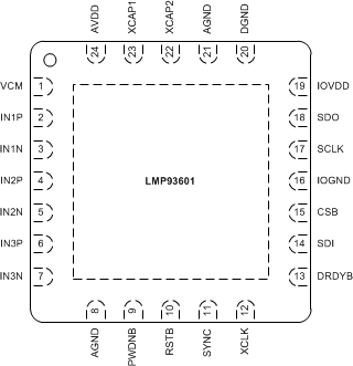
Pin Functions
| PIN(2) | TYPE(I/O)(1) | DESCRIPTION | |
|---|---|---|---|
| NAME | NUMBER | ||
| VCM | 1 | Analog in/output | Sensor common mode bias voltage |
| INP1 | 2 | Analog input | Input signal positive pin |
| INN1 | 3 | Analog input | Input signal negative pin |
| INP2 | 4 | Analog input | Input signal positive pin |
| INN2 | 5 | Analog input | Input signal negative pin |
| INP3 | 6 | Analog input | Input signal positive pin |
| INN3 | 7 | Analog input | Input signal negative pin |
| AGND | 8 | Analog ground | |
| PWDNB | 9 | Digital input | Enable, active low |
| RSTB | 10 | Digital input | Master reset, active low |
| SYNC | 11 | Digital input | Sync, active high |
| XCLK | 12 | Digital input | External clock source |
| DRDYB | 13 | Digital output | Data ready signal, active low, push-pull |
| SDI | 14 | Digital input | Serial data input |
| CSB | 15 | Digital input | Chip select, active low |
| IOGND | 16 | Digital IO ground | |
| SCLK | 17 | Digital input | Serial interface clock |
| SDO | 18 | Digital output | Serial data output; push-pull |
| IOVDD | 19 | Digital IO supply rail | |
| DGND | 20 | Digital ground | |
| AGND | 21 | Analog ground | |
| XCAP2 | 22 | Digital LDO | External Cap2 |
| XCAP1 | 23 | Analog | External Cap1 |
| AVDD | 24 | Analog | Analog supply rail |
(1) There is no pull-up/-down for any digital I/O
(2) For best performance, it is recommended that the DAP is connected to AGND (refer to Mechanical, Packaging and Orderable Information ). All three “GND” connections (AGND, DGND and IOGND) must be connected to system ground and cannot be left floating.