SNVSC78B february 2022 – may 2023 LMQ66410 , LMQ66420 , LMQ66430
PRODUCTION DATA
- 1
- 1 Features
- 2 Applications
- 3 Description
- 4 Revision History
- 5 Device Comparison Table
- 6 Pin Configuration and Functions
- 7 Specifications
-
8 Detailed Description
- 8.1 Overview
- 8.2 Functional Block Diagram
- 8.3
Feature Description
- 8.3.1 Enable, Start-Up, and Shutdown
- 8.3.2 Adjustable Switching Frequency (with RT)
- 8.3.3 Power-Good Output Operation
- 8.3.4 Internal LDO, VCC, and VOUT/FB Input
- 8.3.5 Bootstrap Voltage and VBOOT-UVLO (BOOT Terminal)
- 8.3.6 Output Voltage Selection
- 8.3.7 Spread Spectrum
- 8.3.8 Soft Start and Recovery from Dropout
- 8.3.9 Current Limit and Short Circuit
- 8.3.10 Thermal Shutdown
- 8.3.11 Input Supply Current
- 8.4 Device Functional Modes
-
9 Application and Implementation
- 9.1 Application Information
- 9.2
Typical Application
- 9.2.1 Synchronous Buck Regulator at 400 kHz
- 9.2.2 Design Requirements
- 9.2.3 Detailed Design Procedure
- 9.2.4 Application Curves
- 9.3 Best Design Practices
- 9.4 Power Supply Recommendations
- 9.5 Layout
- 10Device and Documentation Support
- 11Mechanical, Packaging, and Orderable Information
Package Options
Mechanical Data (Package|Pins)
- RXB|14
Thermal pad, mechanical data (Package|Pins)
Orderable Information
9.4 Power Supply Recommendations
The characteristics of the input supply must be compatible with the Specifications found in this data sheet. In addition, the input supply must be capable of delivering the required input current to the loaded regulator. The average input current can be estimated with Equation 14.
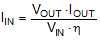
where
- η is the efficiency.
If the regulator is connected to the input supply through long wires or PCB traces, special care is required to achieve good performance. The parasitic inductance and resistance of the input cables can have an adverse effect on the operation of the regulator. The parasitic inductance, in combination with the low-ESR, ceramic input capacitors, can form an underdamped resonant circuit, resulting in overvoltage transients at the input to the regulator. The parasitic resistance can cause the voltage at the VIN pin to dip whenever a load transient is applied to the output. If the application is operating close to the minimum input voltage, this dip can cause the regulator to momentarily shut down and reset. The best way to solve these kinds of issues is to limit the distance from the input supply to the regulator or plan to use an aluminum or tantalum input capacitor in parallel with the ceramics. The moderate ESR of these types of capacitors help dampen the input resonant circuit and reduce any overshoots. A value in the range of 20 µF to 100 µF is usually sufficient to provide input damping and help to hold the input voltage steady during large load transients.
Sometimes, for other system considerations, an input filter is used in front of the regulator. This can lead to instability, as well as some of the effects mentioned above, unless it is designed carefully. The AN-2162 Simple Success With Conducted EMI From DC/DC Converters User's Guide provides helpful suggestions when designing an input filter for any switching regulator.
In some cases, a transient voltage suppressor (TVS) is used on the input of regulators. One class of this device has a snap-back characteristic (thyristor type). The use of a device with this type of characteristic is not recommended. When the TVS fires, the clamping voltage falls to a very low value. If this voltage is less than the output voltage of the regulator, the output capacitors discharge through the device back to the input. This uncontrolled current flow can damage the device.