6 Specifications
6.1 Absolute Maximum Ratings
over operating free-air temperature range (unless otherwise noted) (1)
|
PARAMETER |
MIN |
MAX |
UNIT |
| Input Voltages |
VIN to GND |
-0.3 |
45 |
V |
| SHDN to GND |
-0.3 |
45 |
| FB to GND |
-0.3 |
7 |
| CB to SW |
-0.3 |
7 |
| Output Voltages |
SW to GND |
-1 |
45 |
V |
| SW to GND less than 30ns transients |
-2 |
45 |
| TJ Operation Junction Temperature |
|
-40 |
150 |
°C |
(1) Stresses beyond those listed under Absolute Maximum Ratings may cause permanent damage to the device. These are stress ratings only, which do not imply functional operation of the device at these or any other conditions beyond those indicated under Recommended Operating Conditions. Exposure to absolute-maximum-rated conditions for extended periods may affect device reliability.
6.2 Handling Ratings
|
MIN |
MAX |
UNIT |
| Tstg |
Storage temperature range |
-55 |
165 |
°C |
| V(ESD) |
Electrostatic discharge |
Human body model (HBM), per ANSI/ESDA/JEDEC JS-001, all pins except CB pin(1) |
|
1000 |
V |
| Charged device model (CDM), per JEDEC specification JESD22-C101, all pins(2) |
|
500 |
(1) JEDEC document JEP155 states that 500-V HBM allows safe manufacturing with a standard ESD control process, CB pin passes 500V test.
(2) JEDEC document JEP157 states that 250-V CDM allows safe manufacturing with a standard ESD control process.
6.3 Recommended Operating Conditions (1)
Over operating free-air temperature range (unless otherwise noted)
|
PARAMETER |
MIN |
MAX |
UNIT |
| Buck Regulator |
VIN |
4 |
40 |
V |
| CB |
4 |
46 |
V |
| CB to SW |
-0.3 |
6 |
V |
| SW |
-1 |
40 |
|
| FB |
0 |
5.5 |
V |
| Control |
SHDN |
0 |
40 |
V |
| Temperature |
Operating junction temperature range, TJ |
-40 |
125 |
°C |
6.4 Thermal Information
|
THERMAL METRIC (1) |
TSOT
(6 PINS) |
UNIT |
| RθJA |
Junction-to-ambient thermal resistance |
102 |
°C/W |
| RθJCtop |
Junction-to-case (top) thermal resistance |
36.9 |
| RθJB |
Junction-to board characterization parameter |
28.4 |
(1) All numbers apply for packages soldered directly onto a 3" x 3" PC board with 2 oz. copper on 4 layers in still air in accordance to JEDEC standards. Thermal resistance varies greatly with layout, copper thickness, number of layers in PCB, power distribution, number of thermal vias, board size, ambient temperature, and air flow.
6.5 Electrical Characteristics
VIN = /SHDN = 12V, TA = 25°C, unless otherwise specified.
| SYMBOL |
PARAMETER |
CONDITIONS |
MIN |
TYP |
MAX |
UNIT |
| VIN (Input Power Supply) |
| VIN |
Operating input voltage |
|
4 |
|
40 |
V |
| ISHDN |
Shutdown supply current |
VEN = 0V |
|
1 |
3 |
µA |
| IQ |
Operating quiescent current (non- switching) |
no load, VIN = 12V |
|
28 |
|
µA |
| UVLO |
Undervoltage lockout thresholds |
Rising threshold |
|
|
4 |
V |
| Falling threshold |
3 |
|
|
| SHDN |
| VSHDN_Thre |
Rising SHDN Threshold Voltage |
|
1.05 |
1.25 |
1.38 |
V |
| ISHDN_PIN |
Input current |
SHDN = 2.3V |
|
–4.2 |
|
µA |
| SHDN = 0.9V |
|
–1 |
|
| ISHDN_HYS |
Hysteresis current |
|
|
–3 |
|
µA |
| HIGH-SIDE MOSFET |
|
| RDS_ON |
On-resistance |
VIN = 12V, CB to SW = 5.8V |
|
600 |
|
mΩ |
| VOLTAGE REFERENCE (FB PIN) |
|
| VFB |
Feedback voltage |
|
0.747 |
0.765 |
0.782 |
V |
| CURRENT LIMIT |
| ILIMIT |
Current limit |
VIN = 12V, TJ = 25°C |
|
1200 |
|
mA |
| THERMAL PERFORMANCE |
| TSHDN |
Thermal shutdown threshold |
|
|
170 |
|
ºC |
| THYS |
Hysteresis |
|
|
10 |
|
ºC |
6.6 Switching Characteristics
Over operating free-air temperature range (unless otherwise noted)
| PARAMETER |
TEST CONDITIONS |
MIN |
TYP |
MAX |
UNIT |
| SW (SW PIN) |
| fSW |
Switching frequency |
LMR14006X |
935 |
1100 |
1285 |
kHz |
| LMR14006Y |
1785 |
2100 |
2415 |
| TON_MIN |
Minimum turn-on time |
fSW = 2.1 MHz |
|
95 |
|
ns |
| DMAX |
Maximum duty cycle |
LMR14006X |
|
96% |
|
|
| LMR14006Y |
|
97% |
|
|
6.7 Typical Characteristics
VIN = 12V, TA = 25°C, unless otherwise specified.
| fSW = 2.1 MHz |
VOUT = 12 V |
|
|
|
|
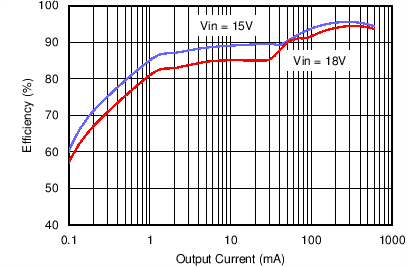
Figure 2. Efficiency vs. Load Current
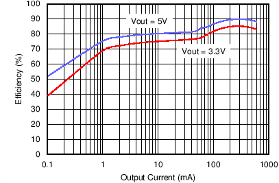 Figure 4. Efficiency vs. Load Current
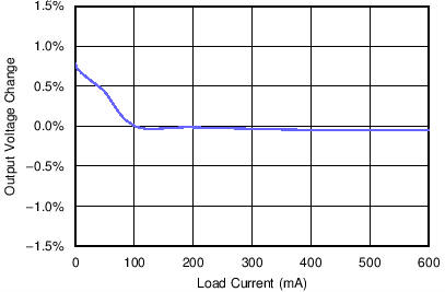 Figure 6. Load Regulation
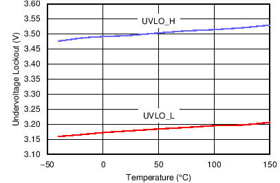 Figure 8. UVLO vs Temperature
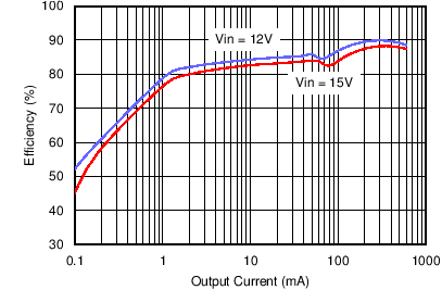 Figure 3. Efficiency vs. Load Current
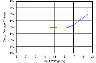 Figure 5. Line Regulation
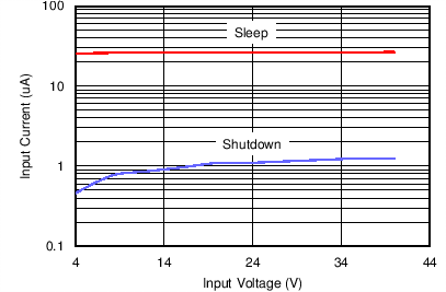 Figure 7. Supply Current vs Input Voltage (No Load)