SNVSBI9A October 2019 – June 2022 LMR33610
PRODUCTION DATA
- 1
- 1 Features
- 2 Applications
- 3 Description
- 4 Revision History
- 5 Device Comparison
- 6 Pin Configuration and Functions
- 7 Specifications
- 8 Detailed Description
-
9 Application and Implementation
- 9.1 Application Information
- 9.2
Typical Application
- 9.2.1 Design Requirements
- 9.2.2
Detailed Design Procedure
- 9.2.2.1 Custom Design With WEBENCH® Tools
- 9.2.2.2 Choosing the Switching Frequency
- 9.2.2.3 Setting the Output Voltage
- 9.2.2.4 Inductor Selection
- 9.2.2.5 Output Capacitor Selection
- 9.2.2.6 Input Capacitor Selection
- 9.2.2.7 CBOOT
- 9.2.2.8 VCC
- 9.2.2.9 CFF Selection
- 9.2.2.10 External UVLO
- 9.2.2.11 Maximum Ambient Temperature
- 9.2.3 Application Curves
- 9.3 What to Do and What Not to Do
- 10Power Supply Recommendations
- 11Layout
- 12Device and Documentation Support
- 13Mechanical, Packaging, and Orderable Information
Package Options
Mechanical Data (Package|Pins)
- DDA|8
Thermal pad, mechanical data (Package|Pins)
- DDA|8
Orderable Information
9.2.2.11 Maximum Ambient Temperature
As with any power conversion device, the LMR33610 dissipates internal power while operating. The effect of this power dissipation is to raise the internal temperature of the converter above ambient. The internal die temperature (TJ) is a function of the ambient temperature, the power loss, and the effective thermal resistance, RθJA, of the device and PCB combination. The maximum internal die temperature for the LMR33610 must be limited to 125°C. This establishes a limit on the maximum device power dissipation and, therefore, the load current. Equation 11 shows the relationships between the important parameters. It is easy to see that larger ambient temperatures (TA) and larger values of RθJA reduce the maximum available output current. The converter efficiency can be estimated by using the curves provided in this data sheet. If the desired operating conditions cannot be found in one of the curves, then interpolation can be used to estimate the efficiency. Alternatively, the EVM can be adjusted to match the desired application requirements and the efficiency can be measured directly. The correct value of RθJA is more difficult to estimate. As stated in the Semiconductor and IC Package Thermal Metrics Application Report, the value of RθJA given in the Thermal Information is not valid for design purposes and must not be used to estimate the thermal performance of the application. The values reported in that table were measured under a specific set of conditions that are rarely obtained in an actual application.
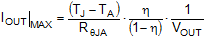
where
- η = efficiency
The effective RθJA is a critical parameter and depends on many factors such as the following:
- Power dissipation
- Air temperature/flow
- PCB area
- Copper heat-sink area
- Number of thermal vias under the package
- Adjacent component placement
The HSOIC (DDA) package uses a die attach paddle or thermal pad (PAD) to provide a place to solder down to the PCB heat-sinking copper. This provides a good heat conduction path from the regulator junction to the heat sink and must be properly soldered to the PCB heat sink copper. Typical examples of RθJA versus copper board area can be found in Figure 9-3. The copper area given in the graph is for each layer; the top and bottom layers are 2-ounce copper each, while the inner layers are 1 ounce.
Figure 9-4 and Figure 9-5 show the typical curves of maximum output current versus ambient temperature. This data was taken with a device and PCB combination, giving an RθJA as noted in the graph. Remember that the data given in these graphs are for illustration purposes only and the actual performance in any given application depends on all of the previously mentioned factors.
 Package")

| VIN = 12 V | VOUT = 5 V | ||
| ƒSW = 400 kHz | RθJA = 50°C/W |

| VIN = 12 V | VOUT = 5 V |
| ƒSW = 400 kHz | RθJA = 30°C/W |
Use the following resources as a guide to optimal thermal PCB design and estimating RθJA for a given application environment:
- Thermal Design by Insight not Hindsight Application Report
- A Guide to Board Layout for Best Thermal Resistance for Exposed Pad Packages Application Report
- Semiconductor and IC Package Thermal Metrics Application Report
- Thermal Design Made Simple with LM43603 and LM43602 Application Report
- PowerPAD™ Thermally Enhanced Package Application Report
- PowerPAD™ Made Easy Application Report
- Using New Thermal Metrics Application Report