SNVSBA8A May   2019  – October 2019 LMR34206-Q1

PRODUCTION DATA.  

  1. Features
  2. Applications
  3. Description
    1.     Device Images
      1. 3.1 Simplified Schematic
  4. Revision History
  5. Device Comparison Table
  6. Pin Configuration and Functions
    1.     Pin Functions
  7. Specifications
    1. 7.1 Absolute Maximum Ratings
    2. 7.2 ESD Ratings
    3. 7.3 Recommended Operating Conditions
    4. 7.4 Thermal Information
    5. 7.5 Electrical Characteristics
    6. 7.6 Timing Requirements
    7. 7.7 System Characteristics
    8. 7.8 Typical Characteristics
  8. Detailed Description
    1. 8.1 Overview
    2. 8.2 Functional Block Diagram
    3. 8.3 Feature Description
      1. 8.3.1 Power-Good Flag Output
      2. 8.3.2 Enable and Start-up
      3. 8.3.3 Current Limit and Short Circuit
      4. 8.3.4 Undervoltage Lockout and Thermal Shutdown
    4. 8.4 Device Functional Modes
      1. 8.4.1 Auto Mode
      2. 8.4.2 Forced PWM Operation
      3. 8.4.3 Dropout
      4. 8.4.4 Minimum Switch On-Time
      5. 8.4.5 Spread Spectrum Operation
  9. Application and Implementation
    1. 9.1 Application Information
    2. 9.2 Typical Application
      1. 9.2.1 Design Requirements
        1. 9.2.1.1 Design Requirements
      2. 9.2.2 Detailed Design Procedure
        1. 9.2.2.1 Choosing the Switching Frequency
        2. 9.2.2.2 Setting the Output Voltage
        3. 9.2.2.3 Inductor Selection
        4. 9.2.2.4 Output Capacitor Selection
        5. 9.2.2.5 Input Capacitor Selection
        6. 9.2.2.6 CBOOT
        7. 9.2.2.7 VCC
        8. 9.2.2.8 External UVLO
        9. 9.2.2.9 Maximum Ambient Temperature
      3. 9.2.3 Application Curves
  10. 10Power Supply Recommendations
  11. 11Layout
    1. 11.1 Layout Guidelines
      1. 11.1.1 Ground and Thermal Considerations
    2. 11.2 Layout Example
  12. 12Device and Documentation Support
    1. 12.1 Device Support
      1. 12.1.1 Development Support
    2. 12.2 Documentation Support
      1. 12.2.1 Related Documentation
    3. 12.3 Receiving Notification of Documentation Updates
    4. 12.4 Support Resources
    5. 12.5 Trademarks
    6. 12.6 Electrostatic Discharge Caution
    7. 12.7 Glossary
  13. 13Mechanical, Packaging, and Orderable Information

Package Options

Mechanical Data (Package|Pins)
Thermal pad, mechanical data (Package|Pins)
Orderable Information

Dropout

The dropout performance of any buck regulator is affected by the RDSON of the power MOSFETs, the DC resistance of the inductor, and the maximum duty cycle that the controller can achieve. As the input voltage is reduced to near the output voltage, the off-time of the high-side MOSFET starts to approach the minimum value. Beyond this point the switching may become erratic and/or the output voltage falls out of regulation. To avoid this problem the LMR34206-Q1 automatically reduces the switching frequency to increase the effective duty cycle and maintain regulation. In this data sheet the dropout voltage is defined as the difference between the input and output voltage when the output has dropped by 1% of its nominal value. Under this condition the switching frequency has dropped to its minimum value of about 140 kHz. Note that the 0.4 V short circuit detection threshold is not activated when in dropout mode. Typical dropout characteristics can be found in Figure 15 and Figure 16.
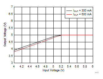
LMR34206-Q1 lmr34206fsc5_voltage_dropout_.gifFigure 15. Overall Dropout Characteristic
VOUT = 5 V
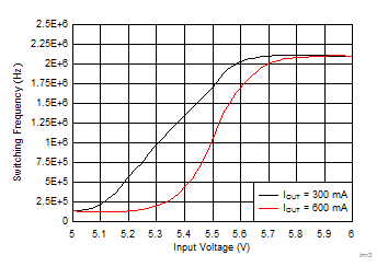
LMR34206-Q1 lmr34206fsc5_frequency_dropout_.gifFigure 16. Typical ƒSW vs Output Current
ƒSW = 2100 kHz