SNVSBD7A October   2019  – February 2020 LMR36510

PRODUCTION DATA.  

  1. Features
  2. Applications
  3. Description
    1.     Device Images
      1.      Efficiency versus Output Current VOUT = 5 V, 400 kHz
      2.      Simplified Schematic
  4. Revision History
  5. Pin Configuration and Functions
    1.     Pin Functions
  6. Specifications
    1. 6.1 Absolute Maximum Ratings
    2. 6.2 ESD Ratings
    3. 6.3 Recommended Operating Conditions
    4. 6.4 Thermal Information
    5. 6.5 Electrical Characteristics
    6. 6.6 Timing Requirements
    7. 6.7 Switching Characteristics
    8. 6.8 System Characteristics
    9. 6.9 Typical Characteristics
  7. Detailed Description
    1. 7.1 Overview
    2. 7.2 Functional Block Diagram
    3. 7.3 Feature Description
      1. 7.3.1 Power-Good Flag Output
      2. 7.3.2 Enable and Start-up
      3. 7.3.3 Current Limit and Short Circuit
      4. 7.3.4 Undervoltage Lockout and Thermal Shutdown
    4. 7.4 Device Functional Modes
      1. 7.4.1 Auto Mode
      2. 7.4.2 Dropout
      3. 7.4.3 Minimum Switch On-Time
  8. Application and Implementation
    1. 8.1 Application Information
    2. 8.2 Typical Application
      1. 8.2.1 Design 1: Low Power 24-V, 1-A Buck Converter
        1. 8.2.1.1 Design Requirements
        2. 8.2.1.2 Detailed Design Procedure
          1. 8.2.1.2.1  Choosing the Switching Frequency
          2. 8.2.1.2.2  Setting the Output Voltage
          3. 8.2.1.2.3  Inductor Selection
          4. 8.2.1.2.4  Output Capacitor Selection
          5. 8.2.1.2.5  Input Capacitor Selection
          6. 8.2.1.2.6  CBOOT
          7. 8.2.1.2.7  VCC
          8. 8.2.1.2.8  CFF Selection
          9. 8.2.1.2.9  External UVLO
          10. 8.2.1.2.10 Maximum Ambient Temperature
      2. 8.2.2 Application Curves
    3. 8.3 What to Do and What Not to Do
  9. Power Supply Recommendations
  10. 10Layout
    1. 10.1 Layout Guidelines
      1. 10.1.1 Ground and Thermal Considerations
    2. 10.2 Layout Example
  11. 11Device and Documentation Support
    1. 11.1 Device Support
      1. 11.1.1 Development Support
    2. 11.2 Documentation Support
      1. 11.2.1 Related Documentation
    3. 11.3 Receiving Notification of Documentation Updates
    4. 11.4 Support Resources
    5. 11.5 Trademarks
    6. 11.6 Electrostatic Discharge Caution
    7. 11.7 Glossary
  12. 12Mechanical, Packaging, and Orderable Information

Package Options

Mechanical Data (Package|Pins)
Thermal pad, mechanical data (Package|Pins)
Orderable Information

Typical Characteristics

Unless otherwise specified the following conditions apply: TA = 25°C and VIN = 24 V.
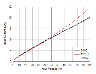
LMR36510 Shutdown_Current.gif
EN = 0 V
Figure 1. Shutdown Supply Current
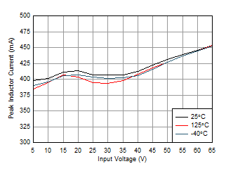
LMR36510 Iminpeak_overVIN.gif
IOUT = 0 A VOUT = 3.3 V ƒSW = 400 kHz
See Figure 34
Figure 2. IPEAK-MIN