SLUSDW3A April 2020 – November 2020 LMR50410
PRODUCTION DATA
- 1 Features
- 2 Applications
- 3 Description
- 4 Revision History
- 5 Device Comparison Table
- 6 Pin Configuration and Functions
- 7 Specifications
- 8 Detailed Description
- 9 Application and Implementation
- 10Power Supply Recommendations
- 11Layout
- 12Device and Documentation Support
- 13Mechanical, Packaging, and Orderable Information
Package Options
Mechanical Data (Package|Pins)
- DBV|6
Thermal pad, mechanical data (Package|Pins)
Orderable Information
8.3.6 Overcurrent and Short Circuit Protection
The LMR50410 incorporates both peak and valley inductor current limit to provide protection to the device from overloads and short circuits and limit the maximum output current. Valley current limit prevents inductor current runaway during short circuits on the output, while both peak and valley limits work together to limit the maximum output current of the converter. Cycle-by-cycle current limit is used for overloads, while hiccup mode is used for sustained short circuits.
High-side MOSFET overcurrent protection is implemented by the nature of the Peak Current Mode control. The high-side switch current is sensed when the high-side is turned on after a set blanking time. The high-side switch current is compared to the output of the Error Amplifier (EA) minus slope compensation every switching cycle. See Section 8.2 for more details. The peak current of high-side switch is limited by a clamped maximum peak current threshold Isc (see Section 7.5), which is constant.
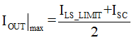
The current going through low-side MOSFET is also sensed and monitored. When the low-side switch turns on, the inductor current begins to ramp down. The low-side switch is not turned OFF at the end of a switching cycle if its current is above the low-side current limit ILS_LIMIT (see Section 7.5). The low-side switch is kept ON so that inductor current keeps ramping down, until the inductor current ramps below the ILS_LIMIT. Then the low-side switch is turned OFF and the high-side switch is turned on after a dead time. After ILS_LIMIT is achieved, peak and valley current limit controls the max current deliver and it can be calculated using Equation 6.
If the feedback voltage is lower than 40% of the VREF, the current of the low-side switch triggers ILS_LIMIT for 256 consecutive cycles and hiccup current protection mode is activated. In hiccup mode, the converter shuts down and keeps off for a period of hiccup, THICCUP (135 ms typical) before the LMR50410 tries to start again. If overcurrent or short-circuit fault condition still exist, hiccup repeats until the fault condition is removed. Hiccup mode reduces power dissipation under severe overcurrent conditions, prevents over-heating and potential damage to the device.
For FPWM version, the inductor current is allowed to go negative. When this current exceed the low-side negative current limit ILS_NEG, the low-side switch is turned off and high-side switch is turned on immediately. This is used to protect the low-side switch from excessive negative current.