SNVSCJ3 December 2023 LMR66410 , LMR66420 , LMR66430
PRODUCTION DATA
- 1
- 1 Features
- 2 Applications
- 3 Description
- 4 Device Comparison Table
- 5 Pin Configuration and Functions
- 6 Specifications
-
7 Detailed Description
- 7.1 Overview
- 7.2 Functional Block Diagram
- 7.3
Feature Description
- 7.3.1 Enable, Start-Up, and Shutdown
- 7.3.2 External CLK SYNC (With MODE/SYNC)
- 7.3.3 Adjustable Switching Frequency (with RT)
- 7.3.4 Power-Good Output Operation
- 7.3.5 Internal LDO, VCC, and VOUT/FB Input
- 7.3.6 Bootstrap Voltage and VBOOT-UVLO (BOOT Terminal)
- 7.3.7 Output Voltage Selection
- 7.3.8 Spread Spectrum
- 7.3.9 Soft Start and Recovery from Dropout
- 7.3.10 Current Limit and Short Circuit
- 7.3.11 Thermal Shutdown
- 7.3.12 Input Supply Current
- 7.4 Device Functional Modes
-
8 Application and Implementation
- 8.1 Application Information
- 8.2
Typical Application
- 8.2.1 Synchronous Buck Regulator at 400 kHz
- 8.2.2 Design Requirements
- 8.2.3 Detailed Design Procedure
- 8.2.4 Application Curves
- 8.3 Best Design Practices
- 8.4 Power Supply Recommendations
- 8.5 Layout
- 9 Device and Documentation Support
- 10Revision History
- 11Mechanical, Packaging, and Orderable Information
Package Options
Mechanical Data (Package|Pins)
- RXB|14
Thermal pad, mechanical data (Package|Pins)
Orderable Information
7.3.1 Enable, Start-Up, and Shutdown
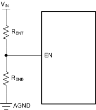
Voltage at the EN pin controls the start-up or remote shutdown of the LMR664x0 family of devices. The part stays shut down as long as the EN pin voltage is less than VEN-WAKE = 0.7 V (typical). During the shutdown, the input current drawn by the device typically drops down to 0.25 µA (VIN = 13.5 V). With the voltage at the EN pin greater than VEN-WAKE, the device enters device standby mode and the internal LDO powers up to generate VCC. As the EN voltage increases further, approaching VEN-VOUT, the device finally starts to switch, entering start-up mode with a soft start. During the device shutdown process, when the EN input voltage measures less than (VEN-VOUT–VEN-HYST), the regulator stops switching and re-enters device standby mode. Any further decrease in the EN pin voltage, below VEN-WAKE, and the device is then firmly shut down. The high-voltage compliant EN input pin can be connected directly to the VIN input pin if remote precision control is not needed. The EN input pin must not be allowed to float. The various EN threshold parameters and the values are listed in the Electrical Characteristics. Figure 7-2 shows the precision enable behavior and Figure 7-3 shows a typical remote EN start-up waveform in an application. After EN goes high, after a delay of about 2.5 ms, the output voltage begins to rise with a soft start and reaches close to the final value in about 3.5 ms (tss). After a delay of about 2.5 ms (tPG_ACT), the PG flag goes high. During start-up, the device is not allowed to enter FPWM mode until the soft-start time has elapsed. This time is measured from the rising edge of EN. Check Section 8.2.3.9 for component selection.
 Figure 7-1 VIN UVLO Using the EN
Pin
 Figure 7-2 Precision Enable
Behavior
 Figure 7-3 Enable Start-Up VIN
= 24 V, VOUT = 3.3 V, IOUT = 2 A