SNVS158E March 2001 – December 2016 LMS33460
PRODUCTION DATA.
- 1 Features
- 2 Applications
- 3 Description
- 4 Revision History
- 5 Pin Configuration and Functions
- 6 Specifications
- 7 Detailed Description
- 8 Application and Implementation
- 9 Power Supply Recommendations
- 10Layout
- 11Device and Documentation Support
- 12Mechanical, Packaging, and Orderable Information
Package Options
Mechanical Data (Package|Pins)
- DCK|5
Thermal pad, mechanical data (Package|Pins)
Orderable Information
8 Application and Implementation
NOTE
Information in the following applications sections is not part of the TI component specification, and TI does not warrant its accuracy or completeness. TI’s customers are responsible for determining suitability of components for their purposes. Customers should validate and test their design implementation to confirm system functionality.
8.1 Application Information
This device is ideal to use in battery-powered or microprocessor based systems and can be used as a low voltage indicator or reset circuit.
8.2 Typical Application
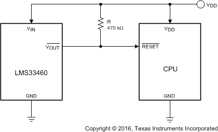
 Figure 8. Typical Application Schematic
8.2.1 Design Requirements
For this design example, use the parameters listed in Table 1 as the input parameters.
Table 1. Design Parameters
| PARAMETER | EXAMPLE VALUE |
|---|---|
| Input supply voltage maximum | 7 V |
| VOUT maximum | 7 V |
| VOUT minimum | 0 V |
| Pullup resistor | 470 kΩ |
8.2.2 Detailed Design Procedure
The LMS33460 is a very easy to use low voltage detector. All that required is the input supply voltage and a pullup resistor at the output. TI recommends 470 kΩ for the pullup resistor.
