SNVS158E March 2001 – December 2016 LMS33460
PRODUCTION DATA.
- 1 Features
- 2 Applications
- 3 Description
- 4 Revision History
- 5 Pin Configuration and Functions
- 6 Specifications
- 7 Detailed Description
- 8 Application and Implementation
- 9 Power Supply Recommendations
- 10Layout
- 11Device and Documentation Support
- 12Mechanical, Packaging, and Orderable Information
Package Options
Mechanical Data (Package|Pins)
- DCK|5
Thermal pad, mechanical data (Package|Pins)
Orderable Information
10 Layout
10.1 Layout Guidelines
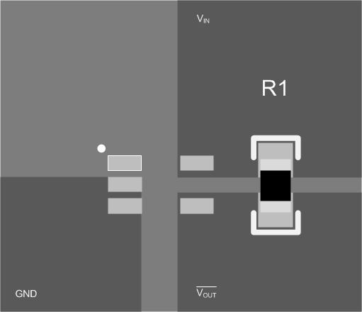
Place the output pullup resistor, and delay capacitor if used, as close as possible to the IC. Keep traces short between the IC and the components used at the output to ensure the timing delay is as accurate as possible.
10.2 Layout Example
 Figure 10. Layout Example Diagram