SNAS714C November 2016 – August 2021 LMS3635-Q1 , LMS3655-Q1
PRODUCTION DATA
- 1 Features
- 2 Applications
- 3 Description
- 4 Revision History
- 5 Device Comparison Tables
- 6 Pin Configuration and Functions
- 7 Specifications
- 8 Detailed Description
-
9 Application and Implementation
- 9.1 Application Information
- 9.2
Typical Applications
- 9.2.1
General Application
- 9.2.1.1 Design Requirements
- 9.2.1.2 Detailed Design Procedure
- 9.2.1.3 Application Curves
- 9.2.2 Fixed 5-V Output for USB-Type Applications
- 9.2.3 Fixed 3.3-V Output
- 9.2.4 6-V Adjustable Output
- 9.2.1
General Application
- 9.3 Do's and Don't's
- 10Power Supply Recommendations
- 11Layout
- 12Device and Documentation Support
- 13Mechanical, Packaging, and Orderable Information
Package Options
Mechanical Data (Package|Pins)
- RNL|22
Thermal pad, mechanical data (Package|Pins)
- RNL|22
Orderable Information
8.3.8 Input Supply Current
The LMS36x5-Q1 is designed to have very low input supply current when regulating light loads. This is achieved by powering much of the internal circuitry from the output. The BIAS pin is the input to the LDO that powers the majority of the control circuits. By connecting the BIAS input to the output of the regulator, this current acts as a small load on the output. This current is reduced by the ratio of VOUT / VIN, just like any other load. Another advantage of the LMS36x5-Q1 is that the feedback divider is integrated into the device. This allows the use of much larger resistors than can be used externally (>> 100 kΩ); this results in much lower divider current than is possible with external resistors.
IQ_VIN is defined as the current consumed by a converter using a LMS3635-Q1 or LMS3655-Q1 device while regulating without a load. To calculate the theoretical total quiescent current, the below equation can be used with parameters from the Section 7.6 and Section 7.7 tables. While operating without a load, the LMS3635-Q1 or LMS3655-Q1 only powers itself. The device draws power from three sources: the VIN pin (IQ), the FB pin (Idiv), and the BIAS pin (IB). Because the BIAS and FB pins are connected to the output of the circuit, the power consumed is converted from input power with an effective efficiency, ηeff, of approximately 80%. Here, effective efficiency is the added input power needed when lightly loading the converter of the LMS3635-Q1 and LMS3655-Q1 devices and is divided by the corresponding additional load. This allows unloaded current to be calculated in Equation 2:
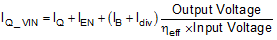
where
- IQ_VIN is the current consumed by the operating (switching) buck converter while unloaded.
- IQ is the current drawn by the LMS36x5-Q1 from its VIN terminal. See IQ in Section 7.6.
- IEN is current drawn by the LMS36x5-Q1 from its EN terminal. Include this current if EN is connected to VIN. See IEN in Section 7.6. Note that this current drops to a very low value if connected to a voltage less than 5 V.
- IB is bias current drawn by the unloaded LMS36x5-Q1. See IB in Section 7.7.
- Idiv is the current drawn by the feedback voltage divider used to set output voltage for adjustable devices. This current is zero for fixed output voltage devices.
- ηeff is the light load efficiency of the Buck converter with IQ_VIN removed from the input current of the buck converter. 0.8 is a conservative value that can be used under normal operating conditions
The EN pin consumes a few micro-amperes when tied to high; see IEN. Add IEN to IQ as shown in Equation 2 if EN is tied to VIN. If EN is tied to a voltage less than 5 V, virtually no current is consumed allowing EN to be used as an UVLO pin once a voltage divider is added.
The Section 9.2.2.3 show measured values for the input supply current for both the 3.3-V and the 5-V output voltage versions.