SLOSE67D june 2020 – april 2023 LMV321A-Q1 , LMV324A-Q1 , LMV358A-Q1
PRODUCTION DATA
- 1 Features
- 2 Applications
- 3 Description
- 4 Revision History
- 5 Pin Configuration and Functions
- 6 Specifications
- 7 Detailed Description
- 8 Application and Implementation
- 9 Power Supply Recommendations
- 10Layout
- 11Device and Documentation Support
- 12Mechanical, Packaging, and Orderable Information
Package Options
Mechanical Data (Package|Pins)
Thermal pad, mechanical data (Package|Pins)
Orderable Information
5 Pin Configuration and Functions
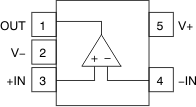
 Figure 5-1 LMV321A-Q1 DBV Package,
5-Pin SOT-23
(Top View)
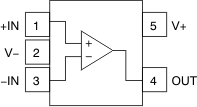
 Figure 5-2 LMV321A-Q1 DCK, LMV321AU-Q1 DBV
Package,
Figure 5-2 LMV321A-Q1 DCK, LMV321AU-Q1 DBV
Package,5-Pin SC70, SOT-23
(Top View)
Table 5-1 Pin Functions:
LMV321A-Q1
| PIN | TYPE(1) | DESCRIPTION | ||
|---|---|---|---|---|
| NAME | DBV | DCK, DBV (U) | ||
| –IN | 4 | 3 | I | Inverting input |
| +IN | 3 | 1 | I | Non-inverting input |
| OUT | 1 | 4 | O | Output |
| V– | 2 | 2 | — | Negative (lowest) supply or ground (for single-supply operation) |
| V+ | 5 | 5 | — | Positive (highest) supply |
(1) I = input, O = output
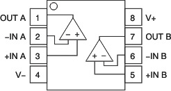
 Figure 5-3 LMV358A-Q1 D and DGK Packages,
8-Pin SOIC and VSSOP
(Top View)
Table 5-2 Pin Functions:
LMV358A-Q1
| PIN | TYPE(1) | DESCRIPTION | |
|---|---|---|---|
| NAME | NO. | ||
| –IN A | 2 | I | Inverting input, channel A |
| +IN A | 3 | I | Non-inverting input, channel A |
| –IN B | 6 | I | Inverting input, channel B |
| +IN B | 5 | I | Non-inverting input, channel B |
| OUT A | 1 | O | Output, channel A |
| OUT B | 7 | O | Output, channel B |
| V– | 4 | — | Negative (lowest) supply or ground (for single-supply operation) |
| V+ | 8 | — | Positive (highest) supply |
(1) I = input, O = output
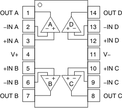
 Figure 5-4 LMV324A-Q1 D, PW, and DYY Packages,
14-Pin SOIC, TSSOP, and SOT-23
(Top View)
Table 5-3 Pin Functions:
LMV324A-Q1
| PIN | TYPE(1) | DESCRIPTION | |
|---|---|---|---|
| NAME | NO. | ||
| –IN A | 2 | I | Inverting input, channel A |
| +IN A | 3 | I | Non-inverting input, channel A |
| –IN B | 6 | I | Inverting input, channel B |
| +IN B | 5 | I | Non-inverting input, channel B |
| –IN C | 9 | I | Inverting input, channel C |
| +IN C | 10 | I | Non-inverting input, channel C |
| –IN D | 13 | I | Inverting input, channel D |
| +IN D | 12 | I | Non-inverting input, channel D |
| OUT A | 1 | O | Output, channel A |
| OUT B | 7 | O | Output, channel B |
| OUT C | 8 | O | Output, channel C |
| OUT D | 14 | O | Output, channel D |
| V– | 11 | — | Negative (lowest) supply or ground (for single-supply operation) |
| V+ | 4 | — | Positive (highest) supply |
(1) I = input, O = output