SNOSAQ5H February 2007 – August 2016 LMV551 , LMV552 , LMV554
PRODUCTION DATA.
- 1 Features
- 2 Applications
- 3 Description
- 4 Revision History
- 5 Pin Configuration and Functions
- 6 Specifications
- 7 Detailed Description
- 8 Application and Implementation
- 9 Power Supply Recommendations
- 10Layout
- 11Device and Documentation Support
- 12Mechanical, Packaging, and Orderable Information
Package Options
Mechanical Data (Package|Pins)
- PW|14
Thermal pad, mechanical data (Package|Pins)
Orderable Information
8 Application and Implementation
NOTE
Information in the following applications sections is not part of the TI component specification, and TI does not warrant its accuracy or completeness. TI’s customers are responsible for determining suitability of components for their purposes. Customers should validate and test their design implementation to confirm system functionality.
8.1 Application Information
The LMV55x have an operating supply voltage range from 2.7 V to 5.5 V. These amplifiers can operate over a wide temperature range (−40°C to 125°C), making them a great choice for automotive applications, sensor applications as well as portable instrumentation applications.
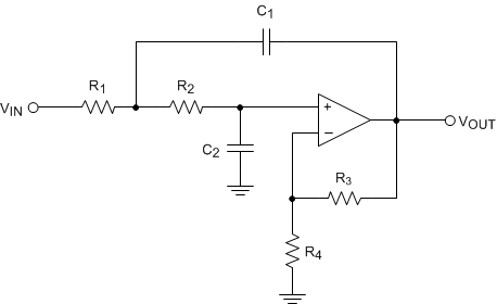
With a wide unity gain bandwidth of 3 MHz, low input referred noise density and an excellent BW to supply current ratio, the LMV55x are well suited for low-power filtering applications. Active filter topologies, such as the Sallen-Key low pass filter shown in Figure 29, are very versatile, and can be used to design a wide variety of filters (Chebyshev, Butterworth or Bessel). For best results, the amplifier must have a bandwidth that is eight to ten times the filter frequency bandwidth. Failure to follow this guideline can result in phase shift of the amplifier and premature roll-off. The Sallen-Key topology, in particular, can be used to attain a wide range of Q, by using positive feedback to reject the undesired frequency range.
8.2 Typical Application
8.2.1 Design Requirements
As a design example:
Require: ALP = 10, less than 1dB passband ripple, and a cutoff frequency of 1kHz.
8.2.2 Detailed Design Procedure
There are many resources discussing the Sallen-Key lowpass filter topology.
Texas Instruments has made filter design easy by creating on-line and stand alone design tools, such as Webench Filter Designer and Filter Pro Desktop.
For this design, the stand-alone Filter Pro Desktop is used.
For the design, the following parameters are entered into the Filterpro software:
- Filter Type = Lowpass
- Gain = 10 V/V (20dB)
- Passband Frequency = 1 kHz
- Allowable Ripple = 1 dB
- Filter Order = Checked and set to 2
- Response Type = Butterworth
- Filter Topology = Sallen-Key
- Component Tolerance - Resistor = E96 1%
- Component Tolerance - Capacitor = E6 20%
After entering these values, FilterPro returns the following recommended values:
- R1 = 44.2 kΩ
- R2 = 38.3 kΩ
- R3 = 2.49 kΩ
- R4 = 22.6 kΩ
- C1 = 10 nF
- C2 = 1.5 nF
The LMV55x is targeted for low power operation. The above resistor values are assumed for a standard power application. To save power, both quiescent and dynamic, the values of the resistors can be increased.
The largest consumer of power is the gain setting feedback resistors R3 and R4, as these are DC coupled and represent a constant DC load to the amplifier. If the output is biased at 2.5 V, then 2.5 V / (22.6 k + 2.49 k) = 99.6 µA is flowing through the feedback network. This is significantly more than the 37uA quiescent current of the amplifier alone! Increasing the size of the feedback resistors by a decade from 22.6k to 226k, the current in the feedback network can be reduced down to 9.9uA.
Increasing the resistor values requires a proportional decrease in the values of the capacitors. If a resistor value is increased 10×, then the corresponding capacitor value must be decreased 10×. However, note that increasing the resistor values increases the contributed noise, and decreasing the capacitors to small values increases the sensitivity to stray capacitance.
There is a decision to be made about also scaling the filter components (R1, R2, C1 & C2). R1 and R2 are AC coupled to the output, so the only DC current flowing through these resistors is the input bias current of the LMV55x (typically 20 nA). However, large AC currents can flow through C2 and C1 during large signal swings. Scaling the filter components also reduces the peak AC signal currents. If the AC signals are expected to large (several Vpp) and frequent, then scaling the filter values may be beneficial to overall power consumption. If the expected AC signals are small, it may not be worth the noise tradeoff to scale these values.
Because the LMV55x has a bipolar input, to maintain DC accuracy, the equivalent resistance seen by each amplifier input should be equal to cancel the bias current effects.
To maintain DC accuracy through bias current cancelling, the following relationship should be maintained:
Fortunately, the filter Pro software makes changing and recalculating the values easy. By changing the value of any of the filter components (R1, R2, C1 & C2) in the schematic tab, the program automatically recalculates and scale these components. Conversely, changing the gain feedback components (R3 or R4) also causes the other feedback resistor to scale. However, Filter Pro does NOT maintain the relationship between the feedback and filter elements as described in Equation 3 above. The feedback resistor values can be 'seeded' and scaled appropriately, as long as the original feedback resistor ratio is maintained.
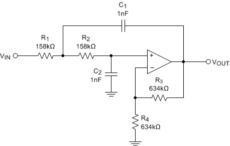
 Figure 30. 1kHz Sallen-Key Low Pass Filter with Values
8.2.3 Application Curve
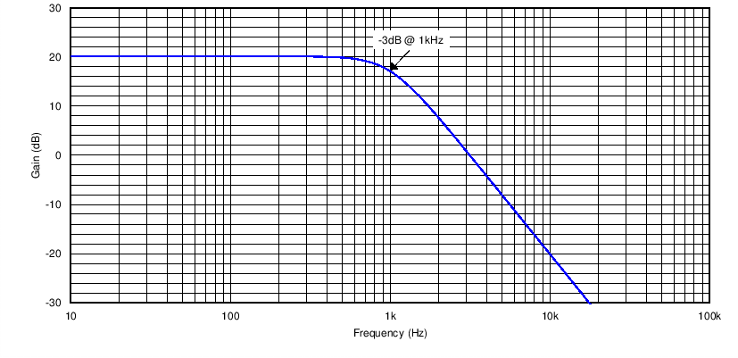
Figure 31 shows the simulated results of the example 1-KHz Sallen-Key Low Pass Filter.

8.3 Do's and Don'ts
Do properly bypass the power supplies.
Do add series resistence to the output when driving capacitive loads, particularly cables, Muxes and ADC inputs.
Do add series current limiting resistors and external Schottky clamp diodes if input voltage is expected to exceed the supplies. Limit the current to 1 mA or less (1 kΩ per volt).
