SNOSAI7K September 2005 – May 2016 LMV651 , LMV652 , LMV654
PRODUCTION DATA.
- 1 Features
- 2 Applications
- 3 Description
- 4 Revision History
- 5 Pin Configuration and Functions
- 6 Specifications
- 7 Detailed Description
- 8 Application and Implementation
- 9 Power Supply Recommendations
- 10Layout
- 11Device and Documentation Support
- 12Mechanical, Packaging, and Orderable Information
Package Options
Mechanical Data (Package|Pins)
- PW|14
Thermal pad, mechanical data (Package|Pins)
Orderable Information
8 Application and Implementation
NOTE
Information in the following applications sections is not part of the TI component specification, and TI does not warrant its accuracy or completeness. TI’s customers are responsible for determining suitability of components for their purposes. Customers should validate and test their design implementation to confirm system functionality.
8.1 Application Information
With a low supply current, low power operation, and low harmonic distortion, the LMV65x devices are ideal for wide-bandwidth, high gain amplification.
8.2 Typical Applications
8.2.1 High Gain, Low Power Inverting Amplifiers
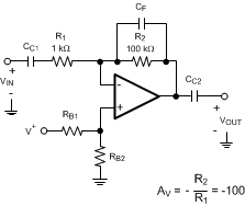
 Figure 37. High Gain Inverting Amplifier
8.2.1.1 Design Requirements
The wide unity-gain bandwidth allows these parts to provide large gain over a wide frequency range, while driving loads as low as 2 kΩ with less than 0.003% distortion.
8.2.1.2 Detailed Design Procedure
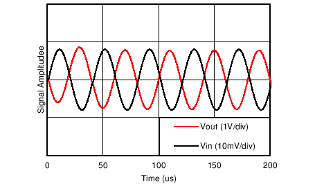
Figure 37 is an inverting amplifier, with a 100-kΩ feedback resistor, R2, and a 1-kΩ input resistor, R1, and provides a gain of −100. With the LMV65x, these circuits can provide gain of −100 with a −3-dB bandwidth of 120 kHz, for a quiescent current as low as 116 μA. Coupling capacitors CC1 and CC2 can be added to isolate the circuit from DC voltages, while RB1 and RB2 provide DC biasing. A feedback capacitor CF can also be added to improve compensation.
8.2.1.3 Application Curve
 Figure 38. High Gain Inverting Amplifier Results
8.2.2 High Gain, Low Power Noninverting Amplifiers
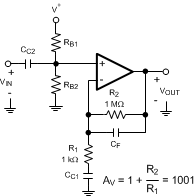
With a low supply current, low power operation, and low harmonic distortion, the LMV65x devices are ideal for wide-bandwidth, high gain amplification. The wide unity-gain bandwidth allows these parts to provide large gain over a wide frequency range, while driving loads as low as 2 kΩ with less than 0.003% distortion. Figure 39 is a noninverting amplifier with a gain of 1001, can provide that gain with a −3-dB bandwidth of 12 kHz, for a similar low quiescent power dissipation. With the LMV65x, these circuits can provide gain of −100 with a −3-dB bandwidth of 120 kHz, for a quiescent current as low as 116 μA. Coupling capacitors CC1 and CC2 can be added to isolate the circuit from DC voltages, while RB1 and RB2 provide DC biasing. A feedback capacitor CF can also be added to improve compensation.
 Figure 39. High Gain Noninverting Amplifier
8.2.3 Active Filters
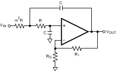
With a wide unity-gain bandwidth of 12 MHz, low input-referred noise density, and a low power supply current, the LMV65x devices are well suited for low-power filtering applications. Active filter topologies, like the Sallen-Key low-pass filter shown in Figure 40, are very versatile, and can be used to design a wide variety of filters (Chebyshev, Butterworth, or Bessel). The Sallen-Key topology, in particular, can be used to attain a wide range of Q, by using positive feedback to reject the undesired frequency range.
In the circuit shown in Figure 40, the two capacitors appear as open circuits at lower frequencies and the signal is simply buffered to the output. At high frequencies the capacitors appear as short circuits and the signal is shunted to ground by one of the capacitors before it can be amplified. Near the cutoff frequency, where the impedance of the capacitances is on the same order as Rg and Rf, positive feedback through the other capacitor allows the circuit to attain the desired Q. The ratio of the two resistors, m2, provides a knob to control the value of Q obtained.
8.3 Dos and Don'ts
Do properly bypass the power supplies.
Do add series resistence to the output when driving capacitive loads, particularly cables, Muxes, and ADC inputs.
Do add series current limiting resistors and external Schottky clamp diodes if input voltage is expected to exceed the supplies. Limit the current to 1 mA or less (1 kΩ per volt).
