SNOS458I April 2000 – June 2016 LMV7219
PRODUCTION DATA.
- 1 Features
- 2 Applications
- 3 Description
- 4 Revision History
- 5 Pin Configuration and Functions
- 6 Specifications
- 7 Detailed Description
- 8 Application and Implementation
- 9 Power Supply Recommendations
- 10Layout
- 11Device and Documentation Support
- 12Mechanical, Packaging, and Orderable Information
Package Options
Mechanical Data (Package|Pins)
Thermal pad, mechanical data (Package|Pins)
Orderable Information
10 Layout
10.1 Layout Guidelines
10.1.1 Circuit Layout and Bypassing
The LMV7219 requires high-speed layout. Follow these layout guidelines:
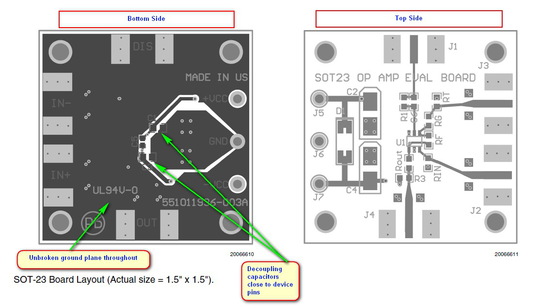
- Power supply bypassing is critical, and will improve stability and eliminate possible output chatter. A decoupling capacitor such as 0.1-µF ceramic should be placed as close as possible to V+ pin (and to V- pin if used with dual supplies) as shown in Figure 20. An additional 2.2-µF tantalum capacitor may be required for extra noise reduction.
- Keep all leads short to reduce stray capacitance and lead inductance. It will also minimize unwanted parasitic feedback around the comparator.
- The device should be soldered directly to the PC board instead of using a socket.
- Use a PC board with a good, unbroken low inductance ground plane as shown in Figure 20. Make sure ground paths are low-impedance, especially were heavier currents are flowing.
- Input traces should be kept away from output traces. This can be achieved by running a topside ground plane between the output and inputs.
- Run the ground trace under the device up to the bypass capacitor to shield the inputs from the outputs.
- To prevent parasitic feedback when input signals are slow-moving, a small capacitor of 1000 pF or less can be placed between the inputs. It can also help eliminate oscillations in the transition region. However, this capacitor can cause some degradation to tpd when the source impedance is low.
10.2 Layout Example
 Figure 20. SOT-23 Board Layout Example