SNOSA56I February 2003 – September 2015 LMV7271 , LMV7272 , LMV7275
PRODUCTION DATA.
- 1 Features
- 2 Applications
- 3 Description
- 4 Revision History
- 5 Pin Configuration and Functions
-
6 Specifications
- 6.1 Absolute Maximum Ratings
- 6.2 ESD Ratings
- 6.3 Recommended Operating Conditions
- 6.4 Thermal Information
- 6.5 1.8-V Electrical Characteristics
- 6.6 1.8-V AC Electrical Characteristics
- 6.7 2.7-V Electrical Characteristics
- 6.8 2.7-V AC Electrical Characteristics
- 6.9 5-V Electrical Characteristics
- 6.10 5-V AC Electrical Characteristics
- 6.11 Typical Characteristics
-
7 Detailed Description
- 7.1 Overview
- 7.2 Functional Block Diagram
- 7.3 Feature Description
- 7.4 Device Functional Modes
- 8 Application and Implementation
- 9 Power Supply Recommendations
- 10Layout
- 11Device and Documentation Support
- 12Mechanical, Packaging, and Orderable Information
Package Options
Mechanical Data (Package|Pins)
Thermal pad, mechanical data (Package|Pins)
Orderable Information
8 Application and Implementation
NOTE
Information in the following applications sections is not part of the TI component specification, and TI does not warrant its accuracy or completeness. TI’s customers are responsible for determining suitability of components for their purposes. Customers should validate and test their design implementation to confirm system functionality.
8.1 Application Information
The LMV727x devices are single-supply comparators with 880 ns of propagation delay and only 12 µA of supply current.
8.2 Typical Applications
8.2.1 Square Wave Oscillator
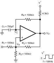 Figure 35. Square Wave Oscillator Application
8.2.1.1 Design Requirements
A typical application for a comparator is as a square wave oscillator. Figure 35 generates a square wave whose period is set by the RC time constant of the capacitor C1and resistor R4. The maximum frequency is limited by the large signal propagation delay of the comparator, and by the capacitive loading at the output, which limits the output slew rate.
8.2.1.2 Detailed Design Procedure
To analyze the circuit, consider it when the output is high. That implies that the inverted input (VC) is lower than the noninverting input (VA).
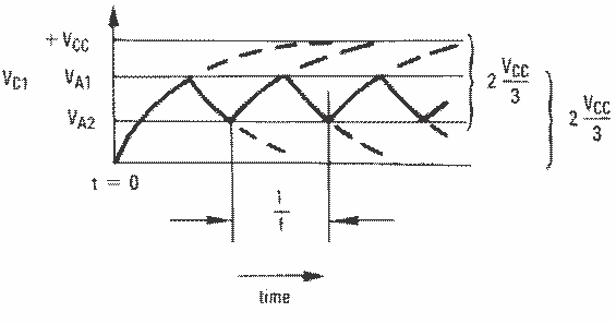 Figure 36. Squarewave Oscillator Timing Thresholds
This causes the C1 to get charged through R4, and the voltage VC increases till it is equal to the noninverting input. The value of VA at this point is

If R1 = R2 = R3, then VA1 = 2VCC/3
At this point the comparator switches pulling down the output to the negative rail. The value of VA at this point is

If R1 = R2 = R3, then VA2 = VCC/3
The capacitor C1 now discharges through R4, and the voltage VC decreases till it is equal to VA2, at which point the comparator switches again, bringing it back to the initial stage. The time period is equal to twice the time it takes to discharge C1 from 2VCC/3 to VCC/3, which is given by R4C1.ln2. Hence the formula for the frequency is:
8.2.1.3 Application Curve
Figure Figure 37 shows the simulated results of an oscillator using the following values:
- R1 = R2 = R3 = R4 = 100 kΩ
- C1 = 750 pF, CL = 20 pF
- V+ = 5 V, V- = GND
- CSTRAY (not shown) from Va to GND = 10 pF
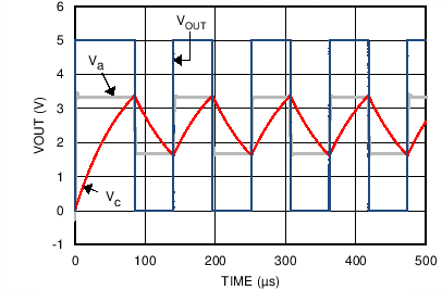 Figure 37. Square Wave Oscillator Output Waveforms
8.2.2 Positive Peak Detector
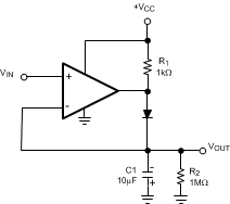 Figure 38. Positive Peak Detector
The positive peak detect circuit is basically a comparator operated in a unity gain follower configuration, with a capacitor as a load to store the highest voltage. A diode is added at the output to prevent the capacitor from discharging through the pullup resistor. When the input VIN increases, the inverting input of the comparator follows it, thus charging the capacitor. When the input voltage decreases, the cap discharges through the 1-MΩ resistor.
The decay time can be modified by changing R2. The output should be accessed through a high-impedance input follower circuit to prevent loading. Upper output swing headroom is determined by the forward voltage of the diode (VMAX = VCC – VF). A Shottky signal diode can be used to reduce the required headroom to around 300 mV.
This circuit can use any of the LMV727x devices, but R1 is not required for the LMV7271 or LMV7272.
8.2.3 Negative Peak Detector
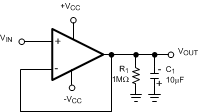 Figure 39. Negative Peak Detector (LMV7275 Only)
The Negative Peak Detector circuit will store the peak negative voltage below ground ( 0 V to –VCC). For the negative detector, the LMV7275 must be used because the output transistor acts as a low-impedance current sink. Because there is no pullup resistor, the only discharge path will be the 1-MΩ resistor and any load impedance used. Decay time is changed by varying the 1-MΩ resistor.
NOTE
The negative peak detector does require a negative supply voltage! +VCC can be grounded to save dynamic range because the output does not swing above ground
8.2.4 Window Detector
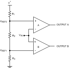 Figure 40. Window Detector
A window detector monitors the input signal to determine if it falls between two voltage levels. Both outputs are true (high) when VREF1 < VIN < VREF2
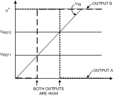 Figure 41. Window Detector Output Signal
The comparator outputs A and B are high only when VREF1 < VIN < VREF2, or within the window, where these are defined as:
To determine if the input signal falls outside of the two voltage levels, both inputs on each comparators can be reversed to invert the logic.
The LMV7275 with an open-drain output should be used if the outputs are to be tied together for a common logic output.
Other names for window detectors are: threshold detector, level detector, and amplitude trigger or detector.