SNOSD49 May 2017 LMV931-N-Q1 , LMV932-N-Q1 , LMV934-N-Q1
PRODUCTION DATA.
- 1 Features
- 2 Applications
- 3 Description
- 4 Revision History
- 5 Pin Configuration and Functions
-
6 Specifications
- 6.1 Absolute Maximum Ratings
- 6.2 ESD Ratings
- 6.3 Recommended Operating Ratings
- 6.4 Thermal Information
- 6.5 DC Electrical Characteristics 1.8 V
- 6.6 AC Electrical Characteristics 1.8 V
- 6.7 DC Electrical Characteristics 2.7 V
- 6.8 AC Electrical Characteristics 2.7 V
- 6.9 Electrical Characteristics 5 V DC
- 6.10 AC Electrical Characteristics 5 V
- 6.11 Typical Characteristics
- 7 Detailed Description
- 8 Application and Implementation
- 9 Power Supply Recommendations
- 10Layout
- 11Device and Documentation Support
- 12Mechanical, Packaging, and Orderable Information
Package Options
Mechanical Data (Package|Pins)
- PW|14
Thermal pad, mechanical data (Package|Pins)
Orderable Information
8 Application and Implementation
NOTE
Information in the following applications sections is not part of the TI component specification, and TI does not warrant its accuracy or completeness. TI’s customers are responsible for determining suitability of components for their purposes. Customers should validate and test their design implementation to confirm system functionality.
8.1 Application Information
The LMV93x-Q1-N devices bring performance, economy and ease-of-use to low-voltage, low-power systems. They provide rail-to-rail input and rail-to-rail output swings into heavy loads.
8.2 Typical Applications
8.2.1 High-Side Current-Sensing Application
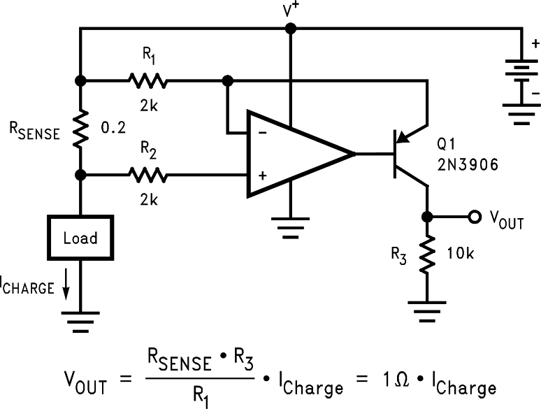 Figure 31. High-Side Current Sensing
8.2.1.1 Design Requirements
The high-side current-sensing circuit (Figure 31) is commonly used in a battery charger to monitor charging current to prevent overcharging. A sense resistor RSENSE is connected to the battery directly. This system requires an op amp with rail-to-rail input. The LMV93x-Q1-N are ideal for this application because its common-mode input range extends up to the positive supply.
8.2.1.1.1 Custom Design With WEBENCH® Tools
Click here to create a custom design using the LMV93x-Q1-N device with the WEBENCH® Power Designer.
- Start by entering the input voltage (VIN), output voltage (VOUT), and output current (IOUT) requirements.
- Optimize the design for key parameters such as efficiency, footprint, and cost using the optimizer dial.
- Compare the generated design with other possible solutions from Texas Instruments.
The WEBENCH Power Designer provides a customized schematic along with a list of materials with real-time pricing and component availability.
In most cases, these actions are available:
- Run electrical simulations to see important waveforms and circuit performance
- Run thermal simulations to understand board thermal performance
- Export customized schematic and layout into popular CAD formats
- Print PDF reports for the design, and share the design with colleagues
Get more information about WEBENCH tools at www.ti.com/WEBENCH.
8.2.1.2 Detailed Design Procedure
As seen in Figure 31, the ICHARGE current flowing through sense resistor RSENSE develops a voltage drop equal to VSENSE. The voltage at the negative sense point will now be less than the positive sense point by an amount proportional to the VSENSE voltage.
The low-bias currents of the LMV93x-Q1-Q1 cause little voltage drop through R2, so the negative input of the LMV93x-Q1 amplifier is at essentially the same potential as the negative sense input.
The LMV93x-Q1 will detect this voltage error between its inputs and servo the transistor base to conduct more current through Q1, increasing the voltage drop across R1 until the LMV93x-Q1 inverting input matches the noninverting input. At this point, the voltage drop across R1 now matches VSENSE.
IG, a current proportional to ICHARGE, will flow according to the following relation:
IG also flows through the gain resistor R3 developing a voltage drop equal to:
where
- G = R3 / R1
The other channel of the LMV93x-Q1 may be used to buffer the voltage across R3 to drive the following stages.
8.2.1.3 Application Curve
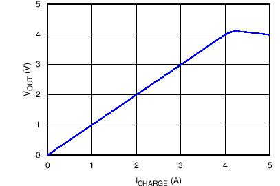
Figure 32 shows the results of the example current sense circuit.
8.2.2 Half-Wave Rectifier Applications
 Figure 33. Half-Wave Rectifier With Rail-To-Ground Output Swing Referenced to Ground
 Figure 34. Half-Wave Rectifier With Negative-Going Output Referenced to VCC
8.2.2.1 Design Requirements
Because the LMV931-N-Q1, LMV932-N-Q1, LMV934-N-Q1 input common-mode range includes both positive and negative supply rails and the output can also swing to either supply, achieving half-wave rectifier functions in either direction is an easy task. All that is needed are two external resistors; there is no need for diodes or matched resistors. The half-wave rectifier can have either positive or negative going outputs, depending on the way the circuit is arranged.
8.2.2.2 Detailed Design Procedure
In Figure 33 the circuit is referenced to ground, while in Figure 34 the circuit is biased to the positive supply. These configurations implement the half-wave rectifier because the LMV93x-Q1-N can not respond to one-half of the incoming waveform. It can not respond to one-half of the incoming because the amplifier cannot swing the output beyond either rail therefore the output disengages during this half cycle. During the other half cycle, however, the amplifier achieves a half wave that can have a peak equal to the total supply voltage. RI should be large enough not to load the LMV93x-Q1-N.
8.2.2.3 Application Curve
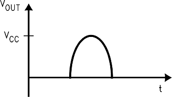 Figure 35. Output of Ground-to-Rail Circuit
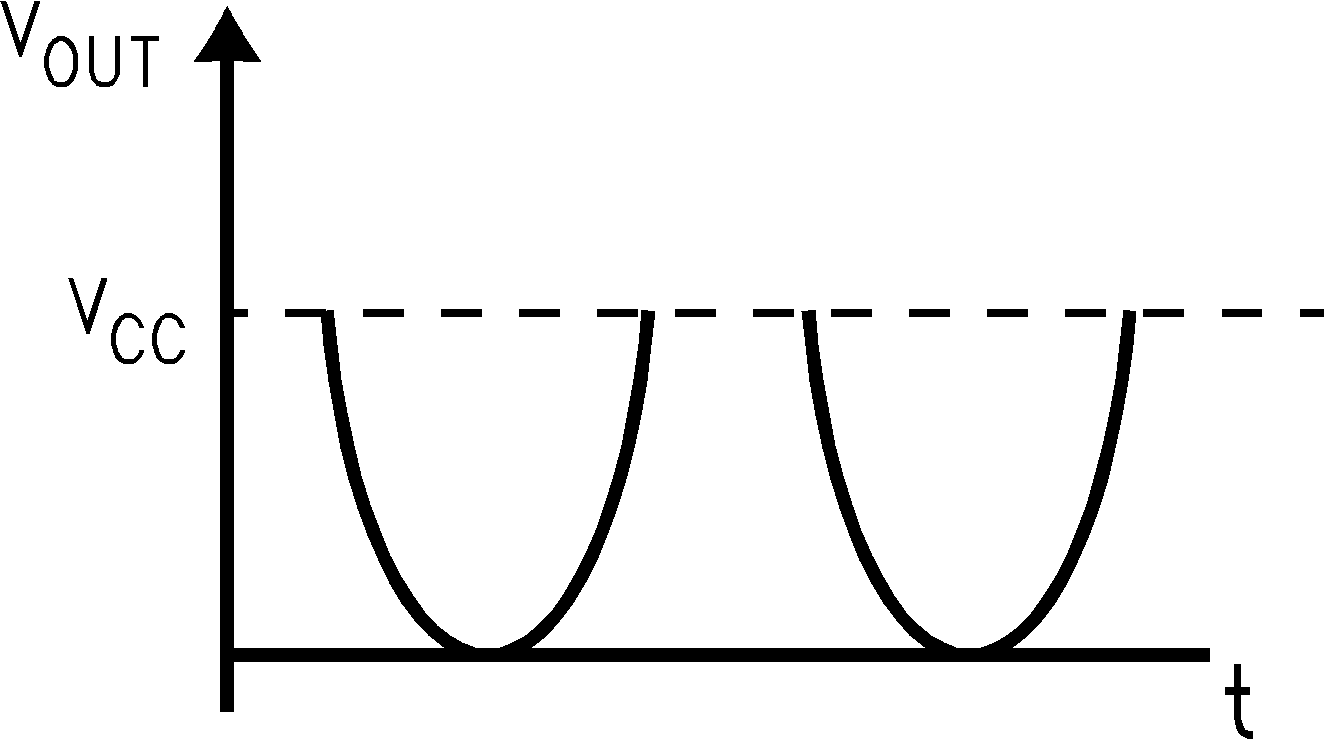 Figure 36. Output of Rail-to-Ground Circuit
8.2.3 Instrumentation Amplifier With Rail-to-Rail Input and Output Application
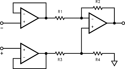 Figure 37. Rail-to-Rail Instrumentation Amplifier
8.2.3.1 Design Requirements
Using three of the LMV93x-Q1-N amplifiers, an instrumentation amplifier with rail-to-rail inputs and outputs can be made as shown in Figure 37.
8.2.3.2 Detailed Design Procedure
In this example, amplifiers on the left side act as buffers to the differential stage. These buffers assure that the input impedance is very high. They also assure that the difference amp is driven from a voltage source. This is necessary to maintain the CMRR set by the matching R1-R2 with R3-R4. The gain is set by the ratio of R2 / R1 and R3 must equal R1 and R4 equal R2. With both rail-to-rail input and output ranges, the input and output are only limited by the supply voltages. Remember that even with rail-to-rail outputs, the output can not swing past the supplies so the combined common-mode voltages plus the signal must not be greater that the supplies or limiting will occur.
8.2.3.3 Application Curve
Figure 38 shows the results of the instrumentation amplifier with R1 and R3 = 1 K, and R2 and R4 = 100 kΩ, for a gain of 100, running on a single 5-V supply with a input of VCM = VS/2. The combined effects of the individual offset voltages can be seen as a shift in the offset of the curve.
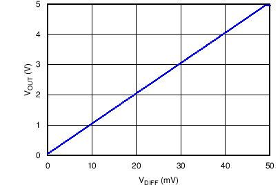 Figure 38. Instrumentation Amplifier Output Results
8.3 Dos and Don'ts
Do properly bypass the power supplies.
Do add series resistence to the output when driving capacitive loads, particularly cables, Muxes and ADC inputs.
Do add series current limiting resistors and external schottky clamp diodes if input voltage is expected to exceed the supplies. Limit the current to 1 mA or less (1 kΩ per volt).