SNVS710I March 2011 – December 2015 LMZ13608
PRODUCTION DATA.
- 1 Features
- 2 Applications
- 3 Description
- 4 Revision History
- 5 Pin Configuration and Functions
- 6 Specifications
- 7 Detailed Description
-
8 Application and Implementation
- 8.1 Application Information
- 8.2
Typical Application
- 8.2.1 Design Requirements
- 8.2.2
Detailed Design Procedure
- 8.2.2.1 Design Steps
- 8.2.2.2 Enable Divider, RENT, RENB and RENH Selection
- 8.2.2.3 Output Voltage Selection
- 8.2.2.4 Soft-Start Capacitor Selection
- 8.2.2.5 Tracking Supply Divider Option
- 8.2.2.6 COUT Selection
- 8.2.2.7 CIN Selection
- 8.2.2.8 Discontinuous Conduction and Continuous Conduction Modes Selection
- 8.2.3 Application Curves
- 9 Power Supply Recommendations
- 10Layout
- 11Device and Documentation Support
- 12Mechanical, Packaging, and Orderable Information
Package Options
Mechanical Data (Package|Pins)
- NDY|11
Thermal pad, mechanical data (Package|Pins)
Orderable Information
7.4.1 Discontinuous Conduction and Continuous Conduction Modes
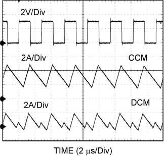
At light load the regulator will operate in discontinuous conduction mode (DCM). With load currents above the critical conduction point, it will operate in continuous conduction mode (CCM). When operating in DCM, inductor current is maintained to an average value equaling IOUT . In DCM the low-side switch will turn off when the inductor current falls to zero, this causes the inductor current to resonate. Although it is in DCM, the current is allowed to go slightly negative to charge the bootstrap capacitor.
In CCM, current flows through the inductor through the entire switching cycle and never falls to zero during the OFF-time.
Figure 46 is a comparison pair of waveforms showing both the CCM (upper) and DCM operating modes.
