SNVS852D June   2012  – August 2018 LMZ20502

PRODUCTION DATA.  

  1. Features
  2. Applications
  3. Description
    1.     Device Images
      1.      Simplified Schematic
      2.      Typical Efficiency for VOUT = 1.8 V Auto Mode
  4. Revision History
  5. Pin Configuration and Functions
    1.     Pin Functions
  6. Specifications
    1. 6.1 Absolute Maximum Ratings
    2. 6.2 ESD Ratings
    3. 6.3 Recommended Operating Conditions
    4. 6.4 Thermal Information
    5. 6.5 Electrical Characteristics
    6. 6.6 System Characteristics
    7. 6.7 Typical Characteristics
  7. Detailed Description
    1. 7.1 Overview
    2. 7.2 Functional Block Diagram
    3. 7.3 Feature Description
      1. 7.3.1 Nano Scale Package
      2. 7.3.2 Internal Synchronous Rectifier
      3. 7.3.3 Current Limit Protection
      4. 7.3.4 Start-Up
      5. 7.3.5 Dropout Behavior
      6. 7.3.6 Power Good Flag Function
      7. 7.3.7 Thermal Shutdown
    4. 7.4 Device Functional Modes
      1. 7.4.1 PWM Operation
      2. 7.4.2 PFM Operation
  8. Application and Implementation
    1. 8.1 Application Information
    2. 8.2 Typical Application
      1. 8.2.1 Detailed Design Procedure
        1. 8.2.1.1 Custom Design With WEBENCH® Tools
        2. 8.2.1.2 Setting The Output Voltage
        3. 8.2.1.3 Output and Feed-Forward Capacitors
        4. 8.2.1.4 Input Capacitors
        5. 8.2.1.5 Maximum Ambient Temperature
        6. 8.2.1.6 Options
      2. 8.2.2 Application Curves
    3. 8.3 Do's and Don'ts
  9. Power Supply Recommendations
  10. 10Layout
    1. 10.1 Layout Guidelines
    2. 10.2 Layout Example
    3. 10.3 Soldering Information
  11. 11Device and Documentation Support
    1. 11.1 Device Support
      1. 11.1.1 Third-Party Products Disclaimer
      2. 11.1.2 Development Support
        1. 11.1.2.1 Custom Design With WEBENCH® Tools
      3. 11.1.3 Documentation Support
        1. 11.1.3.1 Related Documentation
    2. 11.2 Receiving Notification of Documentation Updates
    3. 11.3 Community Resources
    4. 11.4 Trademarks
    5. 11.5 Electrostatic Discharge Caution
    6. 11.6 Glossary
  12. 12Mechanical, Packaging, and Orderable Information
    1. 12.1 Tape and Reel Information

Package Options

Refer to the PDF data sheet for device specific package drawings

Mechanical Data (Package|Pins)
  • SIL|8
Thermal pad, mechanical data (Package|Pins)
Orderable Information

Power Good Flag Function

The operation of the power good flag function is described in the diagram shown in Figure 13.
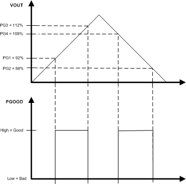
LMZ20502 pgood1_fig26.gifFigure 13. Typical Power Good Flag Operation

This output consists of an open drain NMOS with an Rdson of about 70 Ω. When used, the power good flag should be connected to a logic supply through a pull-up resistor. It can also be pulled-up to either VIN or VOUT, through an appropriate resistor, as desired. If this function is not needed, the PG output should be left floating. The current through this flag pin should be limited to less than 4 mA. A pull-up resistor of ≥1.5 kΩ will satisfy this requirement. When the EN input is pulled low, the PG flag output will also be forced low, assuming a valid input voltage is present at the VIN pin.