SNVS852D June   2012  – August 2018 LMZ20502

PRODUCTION DATA.  

  1. Features
  2. Applications
  3. Description
    1.     Device Images
      1.      Simplified Schematic
      2.      Typical Efficiency for VOUT = 1.8 V Auto Mode
  4. Revision History
  5. Pin Configuration and Functions
    1.     Pin Functions
  6. Specifications
    1. 6.1 Absolute Maximum Ratings
    2. 6.2 ESD Ratings
    3. 6.3 Recommended Operating Conditions
    4. 6.4 Thermal Information
    5. 6.5 Electrical Characteristics
    6. 6.6 System Characteristics
    7. 6.7 Typical Characteristics
  7. Detailed Description
    1. 7.1 Overview
    2. 7.2 Functional Block Diagram
    3. 7.3 Feature Description
      1. 7.3.1 Nano Scale Package
      2. 7.3.2 Internal Synchronous Rectifier
      3. 7.3.3 Current Limit Protection
      4. 7.3.4 Start-Up
      5. 7.3.5 Dropout Behavior
      6. 7.3.6 Power Good Flag Function
      7. 7.3.7 Thermal Shutdown
    4. 7.4 Device Functional Modes
      1. 7.4.1 PWM Operation
      2. 7.4.2 PFM Operation
  8. Application and Implementation
    1. 8.1 Application Information
    2. 8.2 Typical Application
      1. 8.2.1 Detailed Design Procedure
        1. 8.2.1.1 Custom Design With WEBENCH® Tools
        2. 8.2.1.2 Setting The Output Voltage
        3. 8.2.1.3 Output and Feed-Forward Capacitors
        4. 8.2.1.4 Input Capacitors
        5. 8.2.1.5 Maximum Ambient Temperature
        6. 8.2.1.6 Options
      2. 8.2.2 Application Curves
    3. 8.3 Do's and Don'ts
  9. Power Supply Recommendations
  10. 10Layout
    1. 10.1 Layout Guidelines
    2. 10.2 Layout Example
    3. 10.3 Soldering Information
  11. 11Device and Documentation Support
    1. 11.1 Device Support
      1. 11.1.1 Third-Party Products Disclaimer
      2. 11.1.2 Development Support
        1. 11.1.2.1 Custom Design With WEBENCH® Tools
      3. 11.1.3 Documentation Support
        1. 11.1.3.1 Related Documentation
    2. 11.2 Receiving Notification of Documentation Updates
    3. 11.3 Community Resources
    4. 11.4 Trademarks
    5. 11.5 Electrostatic Discharge Caution
    6. 11.6 Glossary
  12. 12Mechanical, Packaging, and Orderable Information
    1. 12.1 Tape and Reel Information

Package Options

Refer to the PDF data sheet for device specific package drawings

Mechanical Data (Package|Pins)
  • SIL|8
Thermal pad, mechanical data (Package|Pins)
Orderable Information

Typical Characteristics

Unless otherwise specified the following conditions apply: VIN = 3.6 V, TA = 25°C.
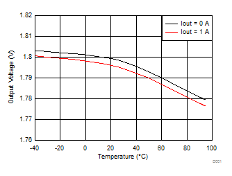
LMZ20502 D001_Tempco_SNVS852.gif
VIN = 3.6 V PWM Mode VOUT = 1.8 V
Figure 1. Typical Output Voltage vs Temperature
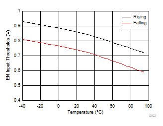
LMZ20502 D003_EN_thresholds_SNVS852.gif
VIN = 3.6 V
Figure 3. EN Input Thresholds
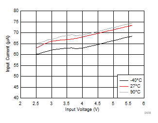
LMZ20502 D005_IQ_auto_SNVS852.gif
VFB = 0.8 V AUTO Mode
Figure 5. Non-Switching Input Current in AUTO Mode
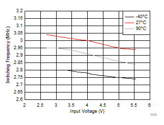
LMZ20502 D002_frequency_SNVS852.gif
VIN = 3.6 V IOUT = 0 A PWM Mode
Figure 2. Switching Frequency in PWM Mode
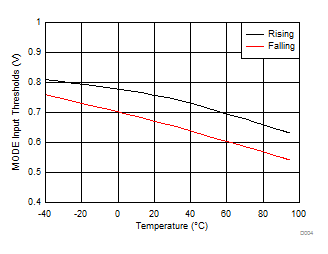
LMZ20502 D004_mode_thresholds_SNVS852.gif
VIN = 3.6 V
Figure 4. MODE Input Thresholds
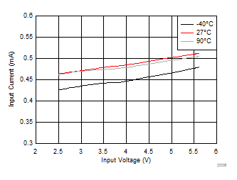
LMZ20502 D006_IQ_pwm_SNVS852.gif
VFB = 0.8 V PWM Mode
Figure 6. Non-Switching Input Current in PWM Mode