SNVS658I March 2011 – August 2015 LMZ22003
PRODUCTION DATA.
- 1 Features
- 2 Applications
- 3 Description
- 4 Revision History
- 5 Pin Configuration and Functions
- 6 Specifications
- 7 Detailed Description
-
8 Application and Implementation
- 8.1 Application Information
- 8.2
Typical Application
- 8.2.1 Design Requirements
- 8.2.2
Detailed Design Procedure
- 8.2.2.1 Design Steps
- 8.2.2.2 Enable Divider, RENT, RENB and RENHSelection
- 8.2.2.3 Output Voltage Selection
- 8.2.2.4 Soft-Start Capacitor Selection
- 8.2.2.5 Tracking Supply Divider Option
- 8.2.2.6 CO Selection
- 8.2.2.7 CIN Selection
- 8.2.2.8 Discontinuous Conduction and Continuous Conduction Modes Selection
- 8.2.3 Application Curves
- 9 Power Supply Recommendations
- 10Layout
- 11Device and Documentation Support
- 12Mechanical, Packaging, and Orderable Information
Package Options
Mechanical Data (Package|Pins)
- NDW|7
Thermal pad, mechanical data (Package|Pins)
Orderable Information
7 Detailed Description
7.1 Overview
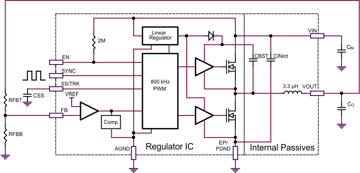
The architecture used is an internally compensated emulated peak current mode control, based on a monolithic synchronous SIMPLE SWITCHER core capable of supporting high load currents. The output voltage is maintained through feedback compared with an internal 0.8-V reference. For emulated peak current-mode, the valley current is sampled on the down-slope of the inductor current. This is used as the DC value of current to start the next cycle.
The primary application for emulated peak current-mode is high input voltage to low output voltage operating at a narrow duty cycle. By sampling the inductor current at the end of the switching cycle and adding an external ramp, the minimum ON-time can be significantly reduced, without the need for blanking or filtering which is normally required for peak current-mode control.
7.2 Functional Block Diagram

7.3 Feature Description
7.3.1 Synchronization Input
The PWM switching frequency can be synchronized to an external frequency source. If this feature is not used, connect this input either directly to ground, or connect to ground through a resistor of 1.5 kΩ or less. The allowed synchronization frequency range is 650 kHz to 950 kHz. The typical input threshold is 1.4-V transition level. Ideally the input clock should overdrive the threshold by a factor of 2, so direct drive from 3.3-V logic through a 1.5-kΩ Thevenin source resistance is recommended.
NOTE
Applying a sustained logic 1 corresponds to zero Hz PWM frequency and will cause the module to stop switching.
7.3.2 Output Over-voltage Protection
If the voltage at FB is greater than a 0.86-V internal reference, the output of the error amplifier is pulled toward ground, causing VO to fall.
7.3.3 Current Limit
The LMZ22003 is protected by both low-side (LS) and high-side (HS) current limit circuitry. The LS current limit detection is carried out during the OFF-time by monitoring the current through the LS synchronous MOSFET. Referring to the Functional Block Diagram, when the top MOSFET is turned off, the inductor current flows through the load, the PGND pin and the internal synchronous MOSFET. If this current exceeds the low-side current limit value, the current limit comparator disables the start of the next switching period. Switching cycles are prohibited until current drops below the limit.
NOTE
DC current limit is dependent on both duty cycle as shown in the graph in the Typical Characteristics section.
The HS current limit monitors the current of top side MOSFET. Once HS current limit is detected, the HS MOSFET is shutoff immediately, until the next cycle. Exceeding HS current limit causes VO to fall. Typical behavior of exceeding LS current limit is that fSW drops to 1/2 of the operating frequency.
7.3.4 Thermal Protection
The junction temperature of the LMZ22003 should not be allowed to exceed its maximum ratings. Thermal protection is implemented by an internal Thermal Shutdown circuit which activates at 165°C (typical) causing the device to enter a low power standby state. In this state the main MOSFET remains off causing VO to fall, and additionally the CSS capacitor is discharged to ground. Thermal protection helps prevent catastrophic failures for accidental device overheating. When the junction temperature falls back below 150°C (typical hysteresis = 15°C) the SS pin is released, VO rises smoothly, and normal operation resumes.
Applications requiring maximum output current especially those at high input voltage may require additional derating at elevated temperatures.
7.3.5 Prebiased Start-Up
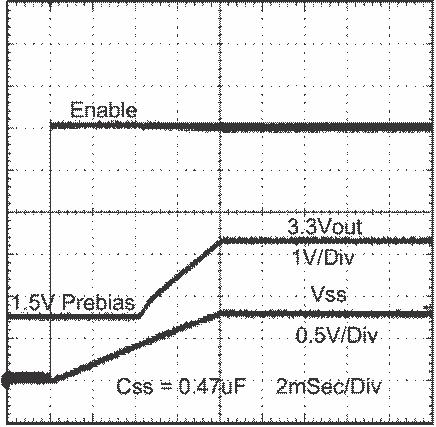
The LMZ22003 will properly start up into a prebiased output. This start-up situation is common in multiple rail logic applications where current paths may exist between different power rails during the start-up sequence. Figure 44 shows proper behavior in this mode. Trace one is Enable going high. Trace two is 1.5-V prebias rising to 3.3 V. Rise-time determined by CSS, trace three.
 Figure 44. Prebiased Start-Up
7.4 Device Functional Modes
7.4.1 Discontinuous Conduction and Continuous Conduction Modes
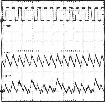
At light load the regulator will operate in discontinuous conduction mode (DCM). With load currents above the critical conduction point, it will operate in continuous conduction mode (CCM). In CCM, current flows through the inductor through the entire switching cycle and never falls to zero during the OFF-time. When operating in DCM, inductor current is maintained to an average value equaling IOUT. Inductor current exhibits normal behavior for the emulated current mode control method used. Output voltage ripple typically increases during this mode of operation.
Figure 45 is a comparison pair of waveforms of the showing both CCM (upper) and DCM operating modes.
