SNVSAJ2C March   2016  – June 2018 LMZ34202

PRODUCTION DATA.  

  1. Features
  2. Applications
  3. Description
    1.     Device Images
      1.      Simplified Application
      2.      Efficiency vs Output Current
  4. Revision History
  5. Pin Configuration and Functions
    1.     Pin Functions
  6. Specifications
    1. 6.1 Absolute Maximum Ratings
    2. 6.2 ESD Ratings
    3. 6.3 Recommended Operating Conditions
    4. 6.4 Thermal Information
    5. 6.5 Electrical Characteristics
    6. 6.6 Switching Characteristics
    7. 6.7 Typical Characteristics
    8. 6.8 Typical Characteristics (Thermal Derating)
  7. Detailed Description
    1. 7.1 Overview
    2. 7.2 Functional Block Diagram
    3. 7.3 Feature Description
      1. 7.3.1  Adjusting the Output Voltage
      2. 7.3.2  Switching Frequency (RT)
      3. 7.3.3  Recommended Operating Range
      4. 7.3.4  Synchronization (CLK)
      5. 7.3.5  Output Capacitor Selection
      6. 7.3.6  VERSA-COMP Pin Configurations
      7. 7.3.7  Input Capacitor Selection
      8. 7.3.8  Output On/Off Inhibit (INH/UVLO)
      9. 7.3.9  Under Voltage Lockout (UVLO)
      10. 7.3.10 Remote Sense
      11. 7.3.11 VBSEL
      12. 7.3.12 Soft-Start (SS/TR)
      13. 7.3.13 Power Good (PWRGD) and Pull-up (PWRGD_PU)
      14. 7.3.14 Overcurrent Protection
      15. 7.3.15 Thermal Shutdown
    4. 7.4 Device Functional Modes
      1. 7.4.1 Active Mode
      2. 7.4.2 Light Load Operation
      3. 7.4.3 Shutdown Mode
  8. Application and Implementation
    1. 8.1 Application Information
    2. 8.2 Typical Application
      1. 8.2.1 Minimum External Component Application
        1. 8.2.1.1 Design Requirements
        2. 8.2.1.2 Detailed Design Procedure
          1. 8.2.1.2.1 Custom Design With WEBENCH® Tools
          2. 8.2.1.2.2 Output Voltage Set-Point
          3. 8.2.1.2.3 RT and RTSEL
          4. 8.2.1.2.4 VERSA-COMP
          5. 8.2.1.2.5 VBSEL
          6. 8.2.1.2.6 Input Capacitors
          7. 8.2.1.2.7 Output Capacitors
        3. 8.2.1.3 Application Curves
      2. 8.2.2 INH Control Application
        1. 8.2.2.1 Design Requirements
      3. 8.2.3 Detailed Design Procedure
        1. 8.2.3.1 Switching Frequency
        2. 8.2.3.2 Power Good
        3. 8.2.3.3 Inhibit Control
        4. 8.2.3.4 VERSA-COMP
        5. 8.2.3.5 VBSEL
        6. 8.2.3.6 Soft-Start Capacitors
        7. 8.2.3.7 Input Capacitors
        8. 8.2.3.8 Output Capacitors
  9. Power Supply Recommendations
  10. 10Layout
    1. 10.1 Layout Guidelines
    2. 10.2 Layout Example
    3. 10.3 EMI
  11. 11Device and Documentation Support
    1. 11.1 Device Support
      1. 11.1.1 Development Support
        1. 11.1.1.1 Custom Design With WEBENCH® Tools
      2. 11.1.2 Third-Party Products Disclaimer
    2. 11.2 Receiving Notification of Documentation Updates
    3. 11.3 Community Resources
    4. 11.4 Trademarks
    5. 11.5 Electrostatic Discharge Caution
    6. 11.6 Glossary
  12. 12Mechanical, Packaging, and Orderable Information
    1. 12.1 Tape and Reel Information

Package Options

Mechanical Data (Package|Pins)
Thermal pad, mechanical data (Package|Pins)
Orderable Information

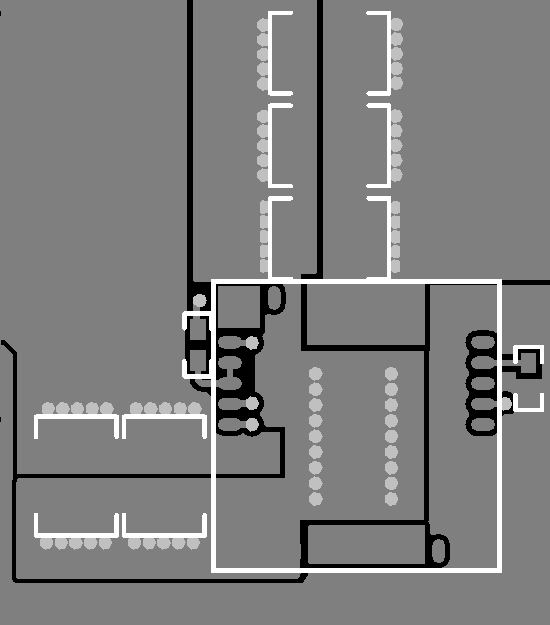
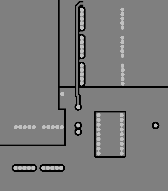
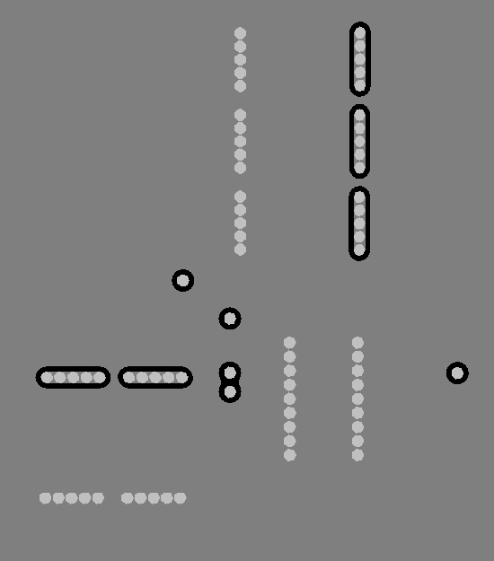
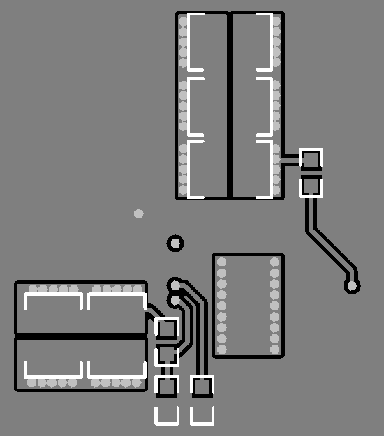
Layout Example

LMZ34202 TOPcrop2.pngFigure 31. Typical Top-Layer Layout
LMZ34202 L3crop2.pngFigure 33. Typical Layer-3 Layout
LMZ34202 L2crop.pngFigure 32. Typical Layer-2 Layout
LMZ34202 BOTcrop.pngFigure 34. Typical Bottom-Layer Layout