SNVSAJ2C March   2016  – June 2018 LMZ34202

PRODUCTION DATA.  

  1. Features
  2. Applications
  3. Description
    1.     Device Images
      1.      Simplified Application
      2.      Efficiency vs Output Current
  4. Revision History
  5. Pin Configuration and Functions
    1.     Pin Functions
  6. Specifications
    1. 6.1 Absolute Maximum Ratings
    2. 6.2 ESD Ratings
    3. 6.3 Recommended Operating Conditions
    4. 6.4 Thermal Information
    5. 6.5 Electrical Characteristics
    6. 6.6 Switching Characteristics
    7. 6.7 Typical Characteristics
    8. 6.8 Typical Characteristics (Thermal Derating)
  7. Detailed Description
    1. 7.1 Overview
    2. 7.2 Functional Block Diagram
    3. 7.3 Feature Description
      1. 7.3.1  Adjusting the Output Voltage
      2. 7.3.2  Switching Frequency (RT)
      3. 7.3.3  Recommended Operating Range
      4. 7.3.4  Synchronization (CLK)
      5. 7.3.5  Output Capacitor Selection
      6. 7.3.6  VERSA-COMP Pin Configurations
      7. 7.3.7  Input Capacitor Selection
      8. 7.3.8  Output On/Off Inhibit (INH/UVLO)
      9. 7.3.9  Under Voltage Lockout (UVLO)
      10. 7.3.10 Remote Sense
      11. 7.3.11 VBSEL
      12. 7.3.12 Soft-Start (SS/TR)
      13. 7.3.13 Power Good (PWRGD) and Pull-up (PWRGD_PU)
      14. 7.3.14 Overcurrent Protection
      15. 7.3.15 Thermal Shutdown
    4. 7.4 Device Functional Modes
      1. 7.4.1 Active Mode
      2. 7.4.2 Light Load Operation
      3. 7.4.3 Shutdown Mode
  8. Application and Implementation
    1. 8.1 Application Information
    2. 8.2 Typical Application
      1. 8.2.1 Minimum External Component Application
        1. 8.2.1.1 Design Requirements
        2. 8.2.1.2 Detailed Design Procedure
          1. 8.2.1.2.1 Custom Design With WEBENCH® Tools
          2. 8.2.1.2.2 Output Voltage Set-Point
          3. 8.2.1.2.3 RT and RTSEL
          4. 8.2.1.2.4 VERSA-COMP
          5. 8.2.1.2.5 VBSEL
          6. 8.2.1.2.6 Input Capacitors
          7. 8.2.1.2.7 Output Capacitors
        3. 8.2.1.3 Application Curves
      2. 8.2.2 INH Control Application
        1. 8.2.2.1 Design Requirements
      3. 8.2.3 Detailed Design Procedure
        1. 8.2.3.1 Switching Frequency
        2. 8.2.3.2 Power Good
        3. 8.2.3.3 Inhibit Control
        4. 8.2.3.4 VERSA-COMP
        5. 8.2.3.5 VBSEL
        6. 8.2.3.6 Soft-Start Capacitors
        7. 8.2.3.7 Input Capacitors
        8. 8.2.3.8 Output Capacitors
  9. Power Supply Recommendations
  10. 10Layout
    1. 10.1 Layout Guidelines
    2. 10.2 Layout Example
    3. 10.3 EMI
  11. 11Device and Documentation Support
    1. 11.1 Device Support
      1. 11.1.1 Development Support
        1. 11.1.1.1 Custom Design With WEBENCH® Tools
      2. 11.1.2 Third-Party Products Disclaimer
    2. 11.2 Receiving Notification of Documentation Updates
    3. 11.3 Community Resources
    4. 11.4 Trademarks
    5. 11.5 Electrostatic Discharge Caution
    6. 11.6 Glossary
  12. 12Mechanical, Packaging, and Orderable Information
    1. 12.1 Tape and Reel Information

Package Options

Mechanical Data (Package|Pins)
Thermal pad, mechanical data (Package|Pins)
Orderable Information

Overcurrent Protection

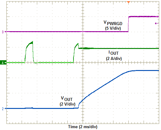
For protection against load faults, the LMZ34202 incorporates output overcurrent protection. Applying a load that exceeds the regulator's overcurrent threshold causes the output to shut down when the output voltage falls below the PWRGD threshold. Following shutdown, the module periodically attempts to recover by initiating a soft-start power-up as shown in Figure 25. This is described as a hiccup mode of operation, whereby the module continues in a cycle of successive shutdown and power up until the load fault is removed. During this period, the average current flowing into the fault is significantly reduced which reduces power dissipation. Once the fault is removed, the module automatically recovers and returns to normal operation as shown in Figure 26.
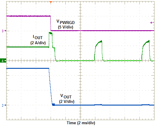
LMZ34202 currentlimiton.pngFigure 25. Overcurrent Limiting
LMZ34202 currentlimitoff.pngFigure 26. Removal of Overcurrent