SNVSA92D September 2015 – June 2018 LMZ36002
PRODUCTION DATA.
- 1 Features
- 2 Applications
- 3 Description
- 4 Revision History
- 5 Pin Configuration and Functions
- 6 Specifications
-
7 Detailed Description
- 7.1 Overview
- 7.2 Functional Block Diagram
- 7.3
Feature Description
- 7.3.1 Adjusting the Output Voltage
- 7.3.2 Switching Frequency (RT)
- 7.3.3 Recommended Operating Range
- 7.3.4 Synchronization (CLK)
- 7.3.5 Output Capacitor Selection
- 7.3.6 VERSA-COMP Pin Configurations
- 7.3.7 Input Capacitor Selection
- 7.3.8 Output On/Off Inhibit (INH/UVLO)
- 7.3.9 Under Voltage Lockout (UVLO)
- 7.3.10 Remote Sense
- 7.3.11 VBSEL
- 7.3.12 Soft-Start (SS/TR)
- 7.3.13 Power Good (PWRGD) and Pull-up (PWRGD_PU)
- 7.3.14 Overcurrent Protection
- 7.3.15 Thermal Shutdown
- 7.4 Device Functional Modes
- 8 Application and Implementation
- 9 Power Supply Recommendations
- 10Layout
- 11Device and Documentation Support
- 12Mechanical, Packaging, and Orderable Information
Package Options
Mechanical Data (Package|Pins)
- RVQ|43
Thermal pad, mechanical data (Package|Pins)
Orderable Information
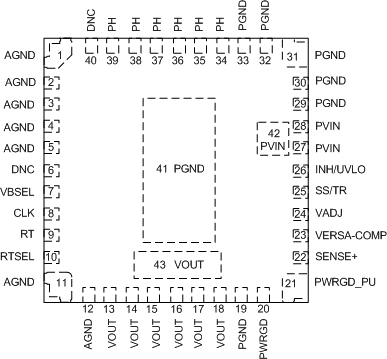
5 Pin Configuration and Functions
RVQ Package
43-Pin QFN
(Top View)

Pin Functions
| PIN | TYPE (1) | DESCRIPTION | |
|---|---|---|---|
| NAME | NO. | ||
| AGND | 1, 2, 3, 4, 5, 11, 12 | G | Zero volt reference for the analog control circuitry. All of these pins are not connected together internal to the device and must be connected to one another externally using an analog ground plane on the PCB. Pins 11 and 12 are internally connected to the PGND of the device at a single point. The analog ground plane of the PCB should allow only analog ground currents to flow through these pins. |
| CLK | 8 | I | Synchronization input to synchronize the device to an external clock. Connect this pin to AGND if not used. |
| DNC | 6, 40 | - | Do Not Connect. Do not connect these pins to AGND, to another DNC pin, or to any other voltage. These pins are connected to internal circuitry. Each pin must be soldered to an isolated pad. |
| INH/UVLO | 26 | I | Inhibit and UVLO adjust pin. Use an open drain or open collector device to control the inhibit function. A resistor divider between this pin, AGND, and PVIN adjusts the UVLO voltage. Connect this pin to PVIN if not used. |
| PGND | 19, 29, 30, 31, 32, 33, 41 | G | This is the return current path for the power stage of the device. Connect these pins to the input source, the load, and to the bypass capacitors associated with PVIN and VOUT using power ground planes on the PCB. Pad 41 should be connected to the ground planes using multiple vias for good thermal performance. |
| PH | 34, 35, 36, 37, 38, 39 | O | Phase switch node. Do not place any external components on these pins or tie them to a pin of another function. |
| PVIN | 27, 28, 42 | I | Power input voltage. These pins supply all of the power to the device. Connect these pins to the input source and connect external bypass capacitors between these pins and PGND close to the device. |
| PWRGD | 20 | O | Power Good flag pin. This open drain output asserts low if the output voltage is more than approximately ±10% out of regulation. This pin is internally connected to an uncommitted 100-kΩ pull-up resistor that can be pulled up to a user-defined voltage applied to the PWRGD_PU pin. |
| PWRGD_PU | 21 | I | An internal 100-kΩ pull-up resistor is connected between this pin and the PWRGD pin. If use of this internal pull-up resistor is desired, connect this pin to an appropriate voltage source that is less than or equal to 12 V. If unused, leave this pin floating. |
| RT | 9 | I | This pin is connected to internal frequency setting circuitry which sets the default switching frequency to 500 kHz. An external resistor can be connected from this pin to AGND to adjust the switching frequency. Refer to application section in datasheet. |
| RTSEL | 10 | I | This pin can be used to adjust the switching frequency to 1 MHz without the need for an external resistor. Connect this pin to AGND to adjust the frequency to 1 MHz. Otherwise, leave this pin floating. |
| SENSE+ | 22 | I | Remote sense connection. This pin must be connected to VOUT at the load or at the device pins. Connect the pin to VOUT at the load for improved regulation. |
| SS/TR | 25 | I | soft-start and tracking pin. Connecting an external capacitor to this pin adjusts the output voltage soft-start ramp above its 4.1 ms default setting. A voltage applied to this pin allows for tracking and sequencing control. |
| VADJ | 24 | I | Connecting a resistor between this pin and AGND adjusts the output voltage. |
| VBSEL | 7 | I | Selectable internal bias supply. For output voltages ≥ 4.5 V, connect this pin to VOUT. For output voltages < 4.5 V, connect this pin to AGND. |
| VERSA-COMP | 23 | I | Connects to internal compensation network. This pin can be left floating or connected to the VADJ pin to select the proper compensation depending on the output voltage. |
| VOUT | 13, 14, 15, 16, 17, 18, 43 | O | Output voltage. These pins are connected to the internal output inductor. Connect these pins to the output load and connect external bypass capacitors between these pins and PGND close to the device. |
(1) G = Ground, I = Input, O = Output