SNVSA92D September   2015  – June 2018 LMZ36002

PRODUCTION DATA.  

  1. Features
  2. Applications
  3. Description
    1.     Device Images
      1.      Simplified Application
      2.      Efficiency vs Output Current
  4. Revision History
  5. Pin Configuration and Functions
    1.     Pin Functions
  6. Specifications
    1. 6.1  Absolute Maximum Ratings
    2. 6.2  ESD Ratings
    3. 6.3  Recommended Operating Conditions
    4. 6.4  Thermal Information
    5. 6.5  Electrical Characteristics
    6. 6.6  Switching Characteristics
    7. 6.7  Typical Characteristics
    8. 6.8  Typical Characteristics
    9. 6.9  Typical Characteristics
    10. 6.10 Typical Characteristics (Thermal Derating)
  7. Detailed Description
    1. 7.1 Overview
    2. 7.2 Functional Block Diagram
    3. 7.3 Feature Description
      1. 7.3.1  Adjusting the Output Voltage
      2. 7.3.2  Switching Frequency (RT)
      3. 7.3.3  Recommended Operating Range
      4. 7.3.4  Synchronization (CLK)
      5. 7.3.5  Output Capacitor Selection
      6. 7.3.6  VERSA-COMP Pin Configurations
      7. 7.3.7  Input Capacitor Selection
      8. 7.3.8  Output On/Off Inhibit (INH/UVLO)
      9. 7.3.9  Under Voltage Lockout (UVLO)
      10. 7.3.10 Remote Sense
      11. 7.3.11 VBSEL
      12. 7.3.12 Soft-Start (SS/TR)
      13. 7.3.13 Power Good (PWRGD) and Pull-up (PWRGD_PU)
      14. 7.3.14 Overcurrent Protection
      15. 7.3.15 Thermal Shutdown
    4. 7.4 Device Functional Modes
      1. 7.4.1 Active Mode
      2. 7.4.2 Light Load Operation
      3. 7.4.3 Shutdown Mode
  8. Application and Implementation
    1. 8.1 Application Information
      1. 8.1.1 Minimum External Component Application
        1. 8.1.1.1 Design Requirements
        2. 8.1.1.2 Detailed Design Procedure
          1. 8.1.1.2.1 Custom Design With WEBENCH® Tools
          2. 8.1.1.2.2 Output Voltage Set-Point
          3. 8.1.1.2.3 RT and RTSEL
          4. 8.1.1.2.4 VERSA-COMP
          5. 8.1.1.2.5 VBSEL
          6. 8.1.1.2.6 Input Capacitors
          7. 8.1.1.2.7 Output Capacitors
          8. 8.1.1.2.8 Application Curves
      2. 8.1.2 Typical Application
        1. 8.1.2.1 Design Requirements
      3. 8.1.3 Detailed Design Procedure
        1. 8.1.3.1 Switching Frequency
        2. 8.1.3.2 Power Good
        3. 8.1.3.3 Inhibit Control
        4. 8.1.3.4 VERSA-COMP
        5. 8.1.3.5 VBSEL
        6. 8.1.3.6 Soft-Start Capacitors
        7. 8.1.3.7 Input Capacitors
        8. 8.1.3.8 Output Capacitors
  9. Power Supply Recommendations
  10. 10Layout
    1. 10.1 Layout Guidelines
    2. 10.2 Layout Example
    3. 10.3 EMI
  11. 11Device and Documentation Support
    1. 11.1 Device Support
      1. 11.1.1 Development Support
        1. 11.1.1.1 Custom Design With WEBENCH® Tools
      2. 11.1.2 Third-Party Products Disclaimer
    2. 11.2 Receiving Notification of Documentation Updates
    3. 11.3 Community Resources
    4. 11.4 Trademarks
    5. 11.5 Electrostatic Discharge Caution
    6. 11.6 Glossary
  12. 12Mechanical, Packaging, and Orderable Information
    1. 12.1 Tape and Reel Information

Package Options

Mechanical Data (Package|Pins)
Thermal pad, mechanical data (Package|Pins)
Orderable Information

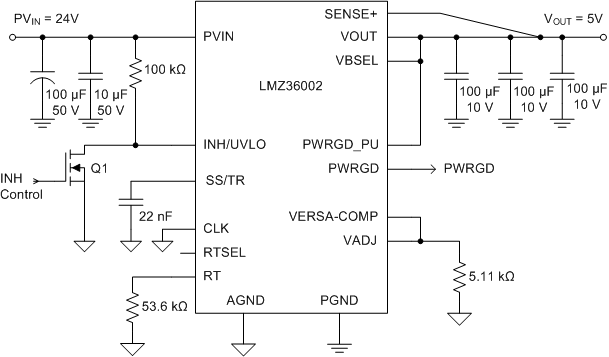
Typical Application

Figure 37 shows a more typical use schematic which makes use of the INH control, Versa-Comp, SS, PWRGD and PWRGD_PU features, along with adjusting the switching frequency with an external resistor. Setting these additional features is described below.
LMZ36002 LMZ36002 Typ App.gifFigure 37. LMZ36002 Typical Schematic