SNVS764Q January 2000 – December 2017 LP2950-N , LP2951-N
PRODUCTION DATA.
- 1 Features
- 2 Applications
- 3 Description
- 4 Revision History
- 5 Voltage Options
- 6 Pin Configuration and Functions
- 7 Specifications
-
8 Detailed Description
- 8.1 Overview
- 8.2 Functional Block Diagrams
- 8.3 Feature Description
- 8.4 Device Functional Modes
-
9 Application and Implementation
- 9.1 Application Information
- 9.2
Typical Applications
- 9.2.1 1-A Regulator with 1.2-V Dropout
- 9.2.2 300-mA Regulator with 0.75-V Dropout
- 9.2.3 Wide Input Voltage Range Current Limiter
- 9.2.4 Low Drift Current Source
- 9.2.5 5-V Current Limiter
- 9.2.6 Regulator with Early Warning and Auxiliary Output
- 9.2.7 Latch Off When Error Flag Occurs
- 9.2.8 2-A Low Dropout Regulator
- 9.2.9 5-V Regulator with 2.5-V Sleep Function
- 9.2.10 Open Circuit Detector for 4 → 20-mA Current Loop
- 9.2.11 Regulator with State-of-Charge Indicator
- 9.2.12 Low Battery Disconnect
- 9.2.13 System Overtemperature Protection Circuit
- 10Power Supply Recommendations
- 11Layout
- 12Device and Documentation Support
- 13Mechanical, Packaging, and Orderable Information
Package Options
Mechanical Data (Package|Pins)
Thermal pad, mechanical data (Package|Pins)
Orderable Information
8 Detailed Description
8.1 Overview
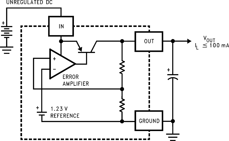
The LP2950-N and LP2951-N are very high accuracy micro power voltage regulators with low quiescent current (75 µA typical) and low dropout voltage (typical 40 mV at light loads and 380 mV at 100 mA). They are ideally suited for use in battery-powered systems.
The LP2950-N and LP2951-N block diagram contains several features, including:
- Very high accuracy 1.23-V reference;
- Fixed 5-V, 3-V, and 3.3-V versions; and
- Internal protection circuitry, such as foldback current limit, and thermal shutdown.
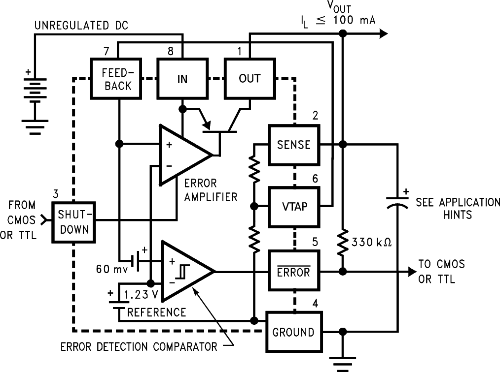
The LP2951-N VERSIONS ONLY:
- Fixed 5-V, 3-V, and 3.3-V versions and programmable output version from 1.24 V to 29 V with an external pair of resistors;
- Shutdown input, allowing turn off the regulator when the SHUTDOWN pin is pulled low; and
- Error flag output, which may be used for a power-on reset.
8.2 Functional Block Diagrams
 Figure 33. LP2950-N Functional Block Diagram
 Figure 34. LP2951-N Functional Block Diagram
8.3 Feature Description
8.3.1 Fixed Voltage Options and Programmable Voltage Version
The LP2950-N and LP2951-N provide 3 fixed output options: 3 V, 3.3 V, and 5 V. Please consult factory for custom voltages. In order to meet different application requirements, LP2951-N can also be used as a programmable voltage regulator, with an external resistors network; please refer to Application and Implementation for more details.
8.3.2 High Accuracy Output Voltage
With special carful design to minimize all contributions to the output voltage error, the LP2950-N/LP2951-N distinguished itself as a very high output voltage accuracy micro power LDO. This includes a tight initial tolerance (0.5% typical), extremely good load and line regulation (.05% typical) and a very low output voltage temperature coefficient, making the part an ideal a low-power voltage reference.
8.3.3 Low Dropout Voltage
Generally speaking, the dropout voltage often refers to the voltage difference between the input and output voltage (VDO = VIN – VOUT), where the main current pass-FET is fully on in the ohmic region of operation and is characterized by the classic RDS(ON) of the FET. VDO indirectly specifies a minimum input voltage above the nominal programmed output voltage at which the output voltage is expected to remain within its accuracy boundary.
8.3.4 Shutdown Mode
When the SHUTDOWN pin is pulled to high level, LP2951-N enters shutdown mode and a very low quiescent current is consumed. This function is designed for the application which needs a shutdown mode to effectively enhance battery life cycle.
8.3.5 Error Detection Comparator Output
The LP2951-N generates a logic low output whenever its output falls out of regulation by more than approximately 5%. Please refer to Application and Implementation for more details.
8.3.6 Internal Protection Circuitry
8.3.6.1 Short-Circuit Protection (Current Limit)
The internal current limit circuit is used to protect the LDO against high-load current faults or shorting events. The LDO is not designed to operate in a steady-state current limit. During a current-limit event, the LDO sources constant current. Therefore, the output voltage falls when load impedance decreases. Note also that if a current limit occurs and the resulting output voltage is low, excessive power may be dissipated across the LDO, resulting in a thermal shutdown of the output. A fold back feature limits the short-circuit current to protect the regulator from damage under all load conditions. If OUT is forced below 0 V before EN goes high and the load current required exceeds the fold back current limit, the device may not start up correctly.
8.3.6.2 Thermal Protection
The device contains a thermal shutdown protection circuit to turn off the output current when excessive heat is dissipated in the LDO. The thermal time-constant of the semiconductor die is fairly short, and thus the output cycles on and off at a high rate when thermal shutdown is reached until the power dissipation is reduced. The internal protection circuitry of the device is designed to protect against thermal overload conditions. The circuitry is not intended to replace proper heat sinking. Continuously running the device into thermal shutdown degrades its reliability.
8.3.7 Enhanced Stability
The LP2950-N and LP2951-N is designed specifically to work with ceramic output capacitors, utilizing circuitry which allows the regulator to be stable across the entire range of output current with an output capacitor whose ESR is as low as 6 mΩ. For output capacitor requirement, please refer to Application and Implementation.
8.4 Device Functional Modes
8.4.1 Operation with 30 V ≥ VIN > VOUT(TARGET) + 1 V
The device operate if the input voltage is equal to, or exceeds VOUT(TARGET) + 1 V. At input voltages below the minimum VIN requirement, the devices do not operate correctly and output voltage may not reach target value.
8.4.2 Operation with Shutdown Control
If the voltage on the SHUTDOWN pin is higher than 1.3 V, the device is disabled. Decreasing shutdown below 0.7 V initiates the start-up sequence of the device.