SNVS764Q January 2000 – December 2017 LP2950-N , LP2951-N
PRODUCTION DATA.
- 1 Features
- 2 Applications
- 3 Description
- 4 Revision History
- 5 Voltage Options
- 6 Pin Configuration and Functions
- 7 Specifications
-
8 Detailed Description
- 8.1 Overview
- 8.2 Functional Block Diagrams
- 8.3 Feature Description
- 8.4 Device Functional Modes
-
9 Application and Implementation
- 9.1 Application Information
- 9.2
Typical Applications
- 9.2.1 1-A Regulator with 1.2-V Dropout
- 9.2.2 300-mA Regulator with 0.75-V Dropout
- 9.2.3 Wide Input Voltage Range Current Limiter
- 9.2.4 Low Drift Current Source
- 9.2.5 5-V Current Limiter
- 9.2.6 Regulator with Early Warning and Auxiliary Output
- 9.2.7 Latch Off When Error Flag Occurs
- 9.2.8 2-A Low Dropout Regulator
- 9.2.9 5-V Regulator with 2.5-V Sleep Function
- 9.2.10 Open Circuit Detector for 4 → 20-mA Current Loop
- 9.2.11 Regulator with State-of-Charge Indicator
- 9.2.12 Low Battery Disconnect
- 9.2.13 System Overtemperature Protection Circuit
- 10Power Supply Recommendations
- 11Layout
- 12Device and Documentation Support
- 13Mechanical, Packaging, and Orderable Information
Package Options
Mechanical Data (Package|Pins)
Thermal pad, mechanical data (Package|Pins)
Orderable Information
11 Layout
11.1 Layout Guidelines
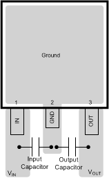
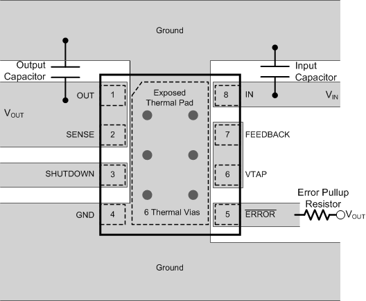
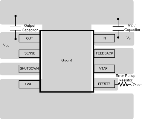
For best overall performance, place all circuit components on the same side of the circuit board and as near as practical to the respective LDO pin connections. Place ground return connections to the input and output capacitor, and to the LDO ground pin as close to each other as possible, connected by a wide, component-side, copper surface. The use of vias and long traces to create LDO circuit connections is strongly discouraged and negatively affects system performance. This grounding and layout scheme minimizes inductive parasitics, and thereby reduces load-current transients, minimizes noise, and increases circuit stability.
A ground reference plane is also recommended and is either embedded in the PCB itself or located on the bottom side of the PCB opposite the components. This reference plane serves to assure accuracy of the output voltage, shield noise, and behaves similar to a thermal plane to spread (or sink) heat from the LDO device. In most applications, this ground plane is necessary to meet thermal requirements.
11.2 Layout Example
 Figure 56. LP2950 Board Layout
 Figure 58. LP2951 WSON Board Layout
 Figure 57. LP2951 VSSOP Board Layout
11.3 WSON Mounting
The NGT (no pullback) 8-lead WSON package requires specific mounting techniques which are detailed in AN-1187 Leadless Leadframe Package (LLP). Referring to the PCB Design Recommendations section, note that the pad style which should be used with the WSON package is the NSMD (non-solder mask defined) type. Additionally, TI recommends that the PCB terminal pads to be 0.2 mm longer than the package pads to create a solder fillet to improve reliability and inspection.
The thermal dissipation of the WSON package is directly related to the printed circuit board construction and the amount of additional copper area connected to the DAP.
For the LP2951-N in the NGT 8-lead WSON package, the junction-to-case thermal rating, RθJC, is 35°C/W, where the case is the bottom of the package at the center of the DAP.
The DAP (exposed pad) on the bottom of the WSON package is connected to the die substrate with a conductive die attach adhesive. The DAP has no direct electrical (wire) connection to any of the eight pins. There is a parasitic PN junction between the die substrate and the device ground. As such, it is strongly recommend that the DAP be connected directly to the ground at device lead 4 (that is, GND). Alternately, but not recommended, the DAP may be left floating (that is, no electrical connection). The DAP must not be connected to any potential other than ground.