SLVSAW6G June 2011 – April 2024 LP2951-Q1
PRODUCTION DATA
- 1
- 1 Features
- 2 Applications
- 3 Description
- 4 Pin Configuration and Functions
- 5 Specifications
- 6 Detailed Description
- 7 Application and Implementation
- 8 Device and Documentation Support
- 9 Revision History
- 10Mechanical, Packaging, and Orderable Information
Package Options
Mechanical Data (Package|Pins)
Thermal pad, mechanical data (Package|Pins)
- DRG|8
Orderable Information
3 Description
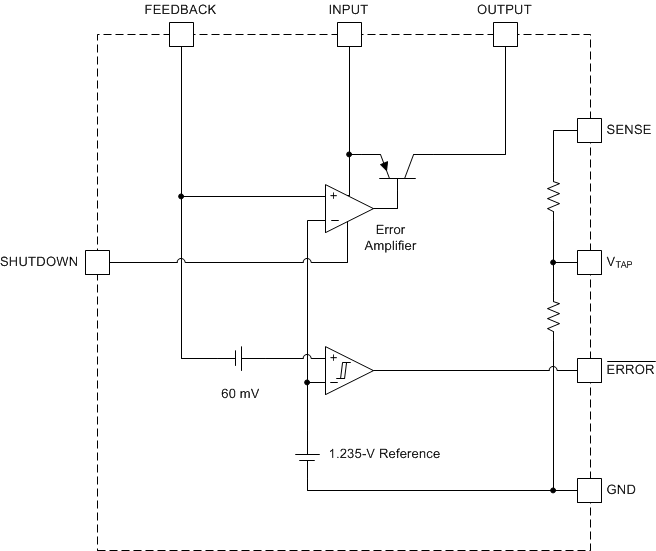
The LP2951-Q1 is a bipolar, low-dropout voltage regulator that can accommodate a wide input supply-voltage range of up to 35V. The 8-pin LP2951-Q1 is able to output either a fixed or adjustable output from the same device. By tying the OUTPUT and SENSE pins together, and the FEEDBACK and VTAP pins together, the LP2951-Q1 outputs a fixed 5V and 3.3V (depending on the version). Alternatively, by leaving the SENSE and VTAP pins open and connecting FEEDBACK to an external resistor divider, the output can be set to any value between 1.235V to 30V.
The LP2951-Q1 device is designed to minimize all error contributions to the output voltage. With a tight output tolerance (0.5% at 25°C), a very low output voltage temperature coefficient (20ppm typical), extremely good line and load regulation (0.3% and 0.4% typical), and remote sensing capability, the device can be used as either a low-power voltage reference or a 100mA regulator.
| PART NUMBER | PACKAGE(1) | PACKAGE SIZE(2) |
|---|---|---|
| LP2951-33-Q1 | DRG (WSON, 8) | 3mm × 3mm |
| LP2951-50-Q1 | ||
| LP2951-50-Q1 | D (SOIC, 8) | 4.9mm × 6mm |
 Simplified Block Diagram