SNVS003G June 1999 – April 2016 LP3470
PRODUCTION DATA.
- 1 Features
- 2 Applications
- 3 Description
- 4 Revision History
- 5 Pin Configuration and Functions
- 6 Specifications
- 7 Detailed Description
- 8 Application and Implementation
- 9 Power Supply Recommendations
- 10Layout
- 11Device and Documentation Support
- 12Mechanical, Packaging, and Orderable Information
Package Options
Mechanical Data (Package|Pins)
- DBV|5
Thermal pad, mechanical data (Package|Pins)
Orderable Information
8 Application and Implementation
NOTE
Information in the following applications sections is not part of the TI component specification, and TI does not warrant its accuracy or completeness. TI’s customers are responsible for determining suitability of components for their purposes. Customers should validate and test their design implementation to confirm system functionality.
8.1 Application Information
The LP3470 is a micropower CMOS voltage supervisor that is ideal for use in battery-powered microprocessor and other digital systems. It is small in size and provides maximum adjustability for power-on-reset (POR) and supervisory functions, making it a good solution in a variety of applications. The LP3470 is available in six standard reset threshold voltage options, and the reset time-out period is adjustable using an external capacitor providing maximum flexibility in any application. This device can ensure system reliability and ensures that a connected microprocessor will operate only when a minimum Vin supply is satisfied.
8.2 Typical Application
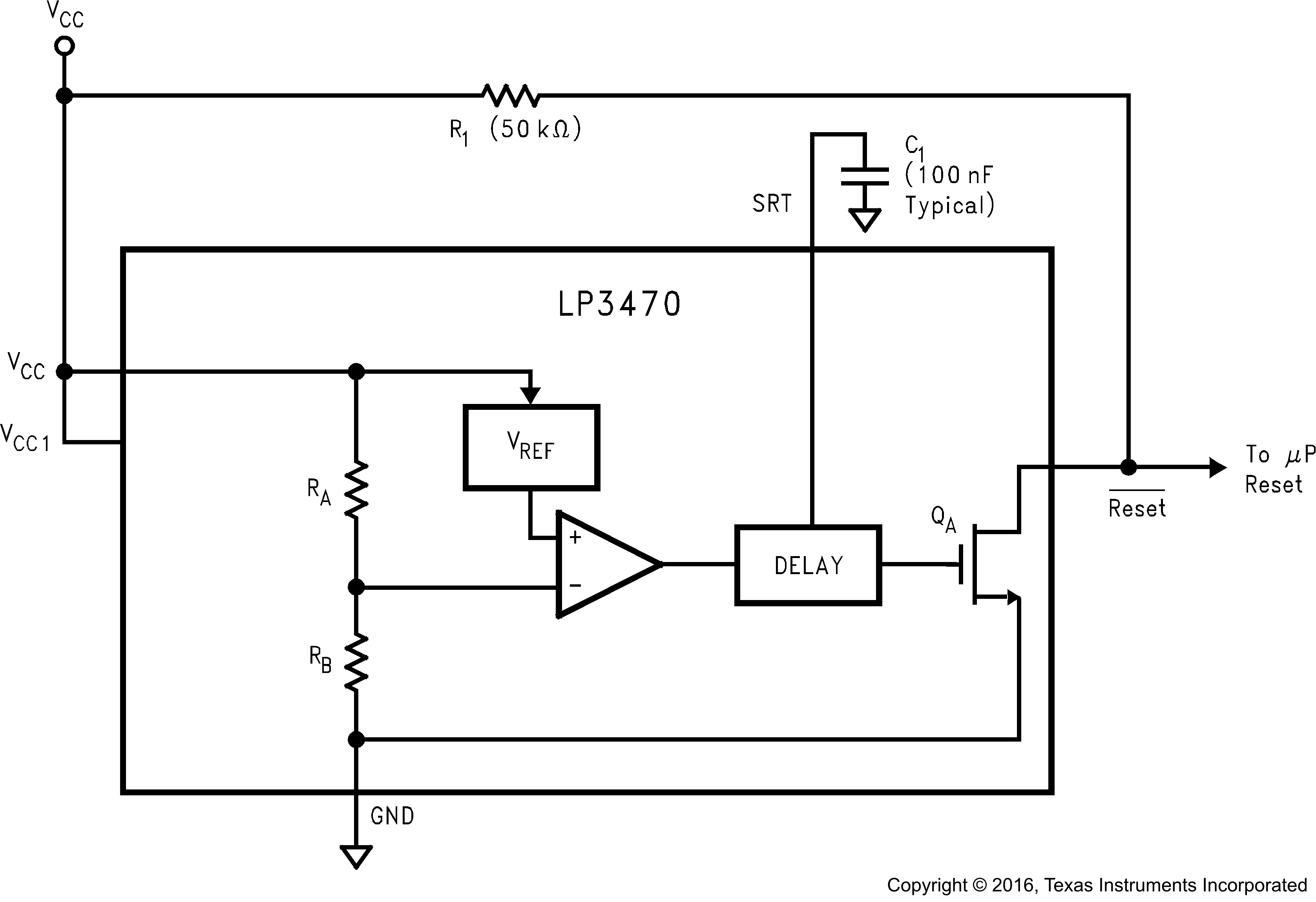
The LP3470 can be used as a simple supervisor circuit to monitor the input supply to a microprocessor as shown in Figure 10.
 Figure 10. Power-On Reset Circuit
8.2.1 Design Requirements
For this design example, use the parameters listed in Table 1 as the input parameters.
Table 1. Design Parameters
| DESIGN PARAMETER | EXAMPLE VALUE |
|---|---|
| Input supply voltage | 0.5 to 5.5 V |
| Reset threshold voltage | 2.63 V, 2.93 V, 3.08 V, 3.65 V, 4 V, 4.38 V, 4.63 V |
| External pullup resistor | 0.68 to 68 kΩ |
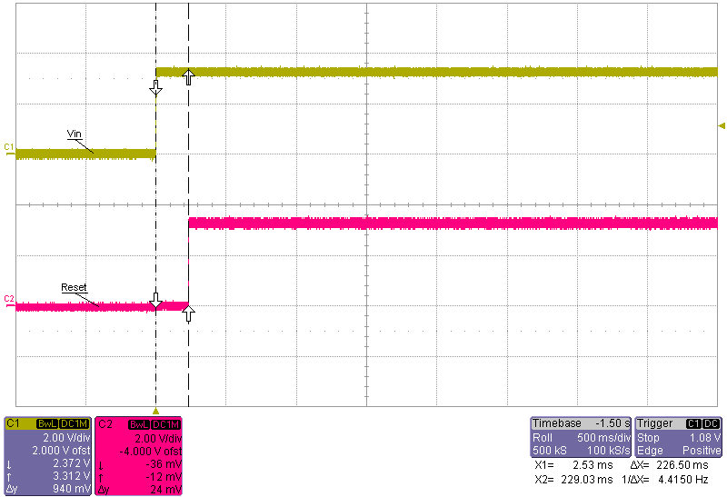
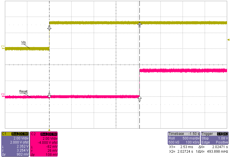
| External reset time-out period capacitor | C1 = 1 nF |
| Reset time-out period | 2 ms |
8.2.2 Detailed Design Procedure
The minimum application circuit requires the LP3470 Power-On Reset Circuit IC and a pullup resistor connecting the reset pin to VCC. The reset delay can be programmed with an additional capacitor connected from the SRT pin to GND. See Reset Time-Out Period and Pullup Resistor Selection for information on choosing specific values for components.

