SNVS003G June   1999  – April 2016 LP3470

PRODUCTION DATA.  

  1. Features
  2. Applications
  3. Description
  4. Revision History
  5. Pin Configuration and Functions
  6. Specifications
    1. 6.1 Absolute Maximum Ratings
    2. 6.2 ESD Ratings
    3. 6.3 Recommended Operating Conditions
    4. 6.4 Thermal Information
    5. 6.5 Electrical Characteristics
    6. 6.6 Typical Characteristics
  7. Detailed Description
    1. 7.1 Functional Block Diagram
    2. 7.2 Feature Description
      1. 7.2.1 Reset Time-Out Period
      2. 7.2.2 Reset Output
      3. 7.2.3 Pullup Resistor Selection
      4. 7.2.4 Negative-Going VCC Transients
    3. 7.3 Device Functional Modes
      1. 7.3.1 Reset Output Low
      2. 7.3.2 Reset Output High
  8. Application and Implementation
    1. 8.1 Application Information
    2. 8.2 Typical Application
      1. 8.2.1 Design Requirements
      2. 8.2.2 Detailed Design Procedure
      3. 8.2.3 Application Curves
  9. Power Supply Recommendations
  10. 10Layout
    1. 10.1 Layout Guidelines
    2. 10.2 Layout Example
  11. 11Device and Documentation Support
    1. 11.1 Community Resources
    2. 11.2 Trademarks
    3. 11.3 Electrostatic Discharge Caution
    4. 11.4 Glossary
  12. 12Mechanical, Packaging, and Orderable Information

Package Options

Mechanical Data (Package|Pins)
Thermal pad, mechanical data (Package|Pins)
Orderable Information

10 Layout

10.1 Layout Guidelines

  • Place components as close as possible to the IC
  • Keep traces short between the IC and the C1 capacitor to ensure the timing delay is as accurate as possible.
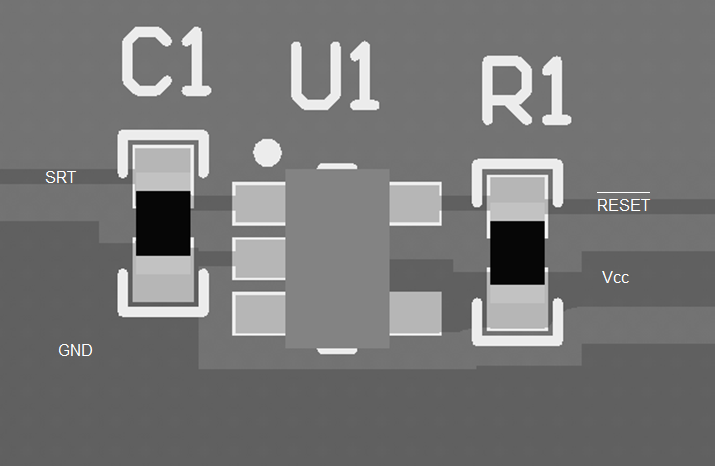
10.2 Layout Example

Figure 13 shows a layout example.

LP3470 layout example.png Figure 13. LP3470 Layout Example