SNVS087AE October 2000 – May 2015 LP3985
PRODUCTION DATA.
- 1 Features
- 2 Applications
- 3 Description
- 4 Revision History
- 5 Pin Configuration and Functions
- 6 Specifications
- 7 Detailed Description
- 8 Application and Implementation
- 9 Power Supply Recommendations
- 10Layout
- 11Device and Documentation Support
- 12Mechanical, Packaging, and Orderable Information
Package Options
Mechanical Data (Package|Pins)
Thermal pad, mechanical data (Package|Pins)
Orderable Information
6 Specifications
6.1 Absolute Maximum Ratings
over operating free-air temperature range (unless otherwise noted) (1)(2)(3)| MIN | MAX | UNIT | ||
|---|---|---|---|---|
| IN, EN | –0.3 | 6.5 | V | |
| OUT | −0.3 | (VIN + 0.3) < 6.5 | ||
| Junction temperature | 150 | °C | ||
| Lead temperature | 235 | |||
| Pad temperature(4) | 235 | |||
| Maximum power dissipation | SOT-23(5) | 364 | mW | |
| DSBGA(5) | 314 | |||
| Storage temperature, Tstg | –65 | 150 | °C | |
(1) Stresses beyond those listed under Absolute Maximum Ratings may cause permanent damage to the device. These are stress ratings only, which do not imply functional operation of the device at these or any other conditions beyond those indicated under Recommended Operating Conditions. Exposure to absolute-maximum-rated conditions for extended periods may affect device reliability.
(2) All voltages are with respect to potential at the GND pin.
(3) If Military/Aerospace specified devices are required, please contact the Texas Instruments Sales Office/ Distributors for availability and specifications.
(4) Additional information on lead temperature and pad temperature can be found in Texas Instruments Application Note AN-1187 Leadless Leadframe Package (LLP) (SNOA401).
(5) The Absolute Maximum power dissipation depends on the ambient temperature and can be calculated using the formula: PD = (TJ - TA)/RθJA,where TJ is the junction temperature, TA is the ambient temperature, and RθJA is the junction-to-ambient thermal resistance. The 364-mW rating for SOT23-5 appearing under Absolute Maximum Ratings results from substituting the Absolute Maximum junction temperature, 150°C for TJ, 70°C for TA, and 220°C/W for RθJA. More power can be dissipated safely at ambient temperatures below 70°C . Less power can be dissipated safely at ambient temperatures above 70°C. The Absolute Maximum power dissipation can be increased by 4.5 mW for each degree below 70°C, and it must be derated by 4.5 mW for each degree above 70°C.
6.2 ESD Ratings
| VALUE | UNIT | |||
|---|---|---|---|---|
| V(ESD) | Electrostatic discharge | Human-body model (HBM), per ANSI/ESDA/JEDEC JS-001(1) | ±2000 | V |
(1) JEDEC document JEP155 states that 500-V HBM allows safe manufacturing with a standard ESD control process.
6.3 Recommended Operating Conditions
over operating free-air temperature range (unless otherwise noted)| MIN | MAX | UNIT | |||
|---|---|---|---|---|---|
| VIN | Supply input voltage | 2.5(1) | 6 | V | |
| VEN | ON/OFF input voltage | 0 | VIN | V | |
| IOUT | Output current | 150 | mA | ||
| TJ | Operating junction temperature | −40 | 125 | °C | |
(1) Recommended minimum VIN is the greater of 2.5-V or VOUT(MAX) + rated dropout voltage (max) for operating load current.
6.4 Thermal Information
| THERMAL METRIC(1) | LP3985 | UNIT | ||
|---|---|---|---|---|
| SOT-23 (DBV) | DSBGA (YZR) | |||
| 5 PINS | ||||
| RθJA | Junction-to-ambient thermal resistance | 220 | 255 | °C/W |
| RθJC(top) | Junction-to-case (top) thermal resistance | 79.8 | 0.8 | |
| RθJB | Junction-to-board thermal resistance | 31.6 | 107.9 | |
| ψJT | Junction-to-top characterization parameter | 3.1 | 0.5 | |
| ψJB | Junction-to-board characterization parameter | 31.1 | 107.9 | |
| RθJC(bot) | Junction-to-case (bottom) thermal resistance | N/A | N/A | |
(1) For more information about traditional and new thermal metrics, see the IC Package Thermal Metrics application report, SPRA953.
6.5 Electrical Characteristics
Unless otherwise specified: VIN = VOUT(nom) + 0.5 V, CIN = 1 μF, IOUT = 1 mA, COUT = 1 μF, CBYPASS = 0.01 μF. Minimum (MIN) and Maximum (MAX) values apply over –40°C ≤ TJ ≤ 125°C and typical values are TA = 25°C, unless otherwise indicated. (1)(2)| PARAMETER | TEST CONDITIONS | MIN | TYP | MAX | UNIT | |
|---|---|---|---|---|---|---|
| ΔVOUT | Output voltage tolerance | IOUT = 1 mA | –2(3)
–3 |
2(3)
3 |
% of VOUT(nom) | |
| Line regulation error | VIN = (VOUT(nom) + 0.5 V) to 6 V, For 4.7-V to 5-V options For all other options |
–0.19 –0.1 |
0.19 0.1 |
%/V | ||
| Load regulation error(4) | IOUT = 1 mA to 150 mA LP3985IM5 (SOT23-5) |
0.0025 | 0.005 | %/mA | ||
| LP3985 (DSBGA) | 0.0004 | 0.002 | %/mA | |||
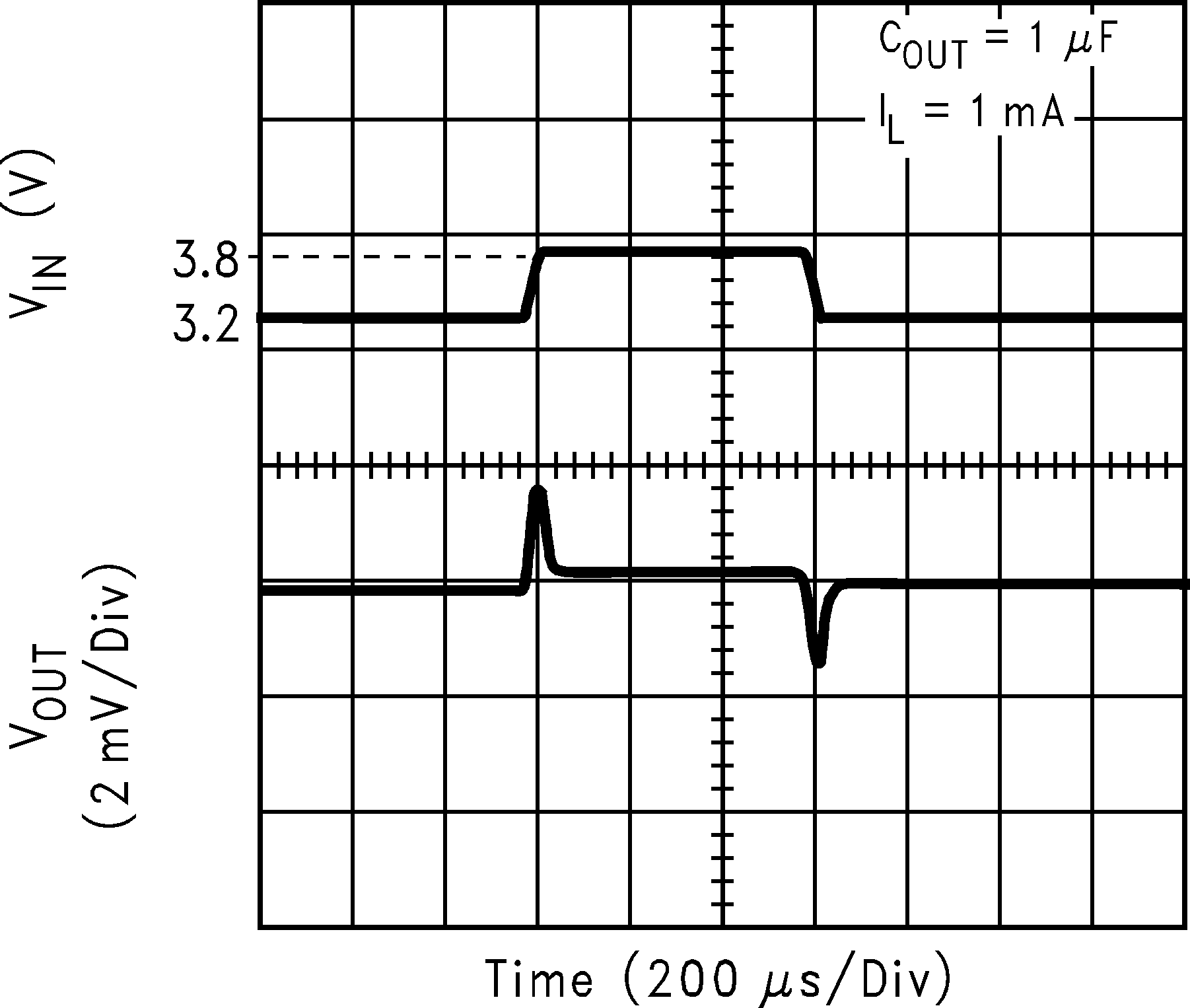
| Output AC line regulation | VIN = VOUT(nom) + 1 V, IOUT = 150 mA (Figure 1) |
1.5 | mVP-P | |||
| PSRR | Power supply rejection ratio | VIN = VOUT(nom) + 0.2 V, f = 1 kHz, IOUT = 50 mA (Figure 2) |
50 | dB | ||
| VIN = VOUT(nom) + 0.2 V, ƒ = 10 kHz, IOUT = 50 mA (Figure 2) |
40 | dB | ||||
| IQ | Quiescent current | VEN = 1.4 V, IOUT = 0 mA For 4.7-V to 5-V options For all other options |
100 85 |
165 150 |
µA | |
| VEN = 1.4 V, IOUT = 0 to 150 mA For 4.7-V to 5-V options For all other options |
155 140 |
250 200 |
||||
| VEN = 0.4 V | 0.003 | 1.5 | ||||
| Dropout voltage(5) | IOUT = 1 mA | 0.4 | 2 | mV | ||
| IOUT = 50 mA | 20 | 35 | mV | |||
| IOUT = 100 mA | 45 | 70 | mV | |||
| IOUT = 150 mA | 60 | 100 | mV | |||
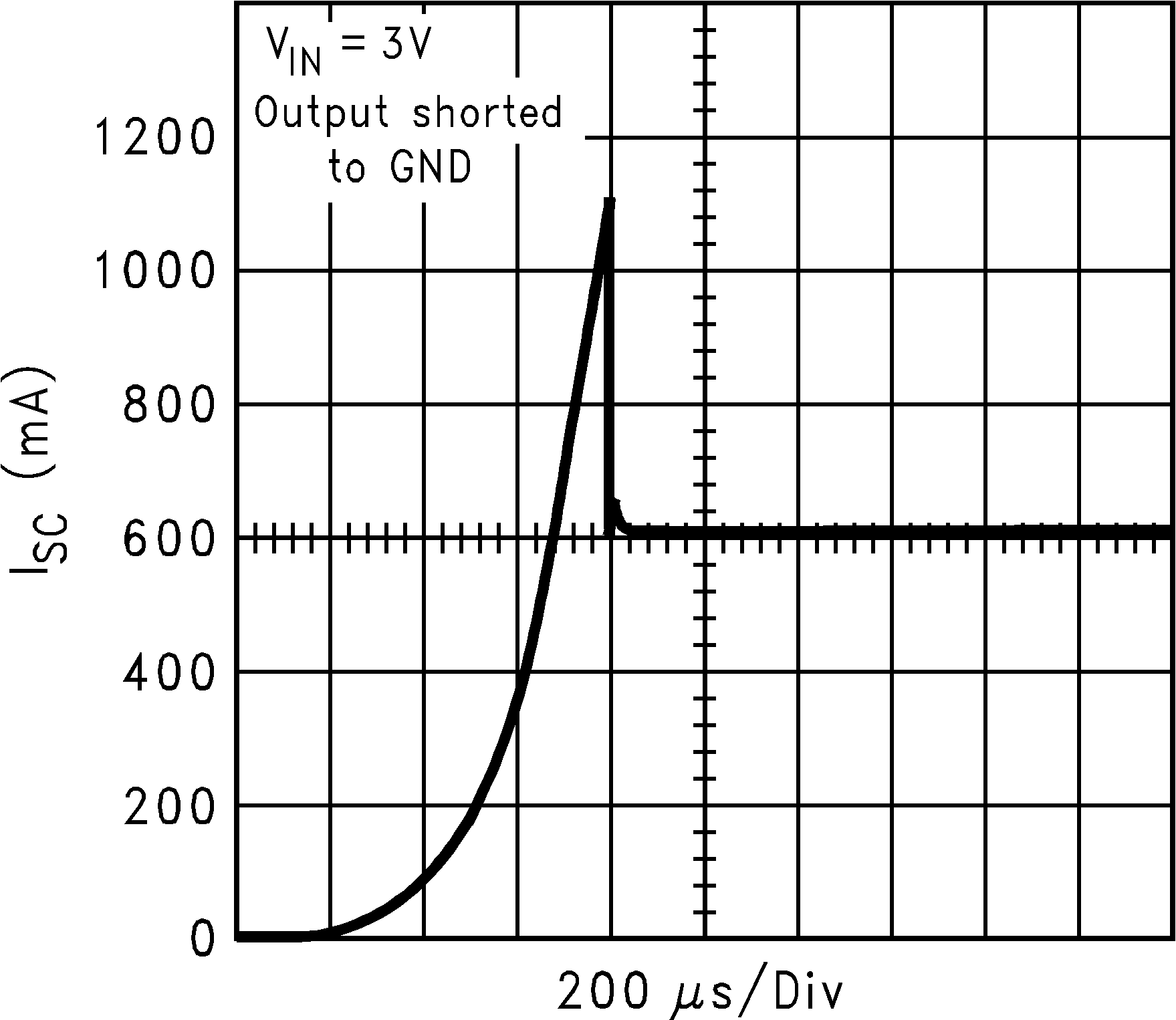
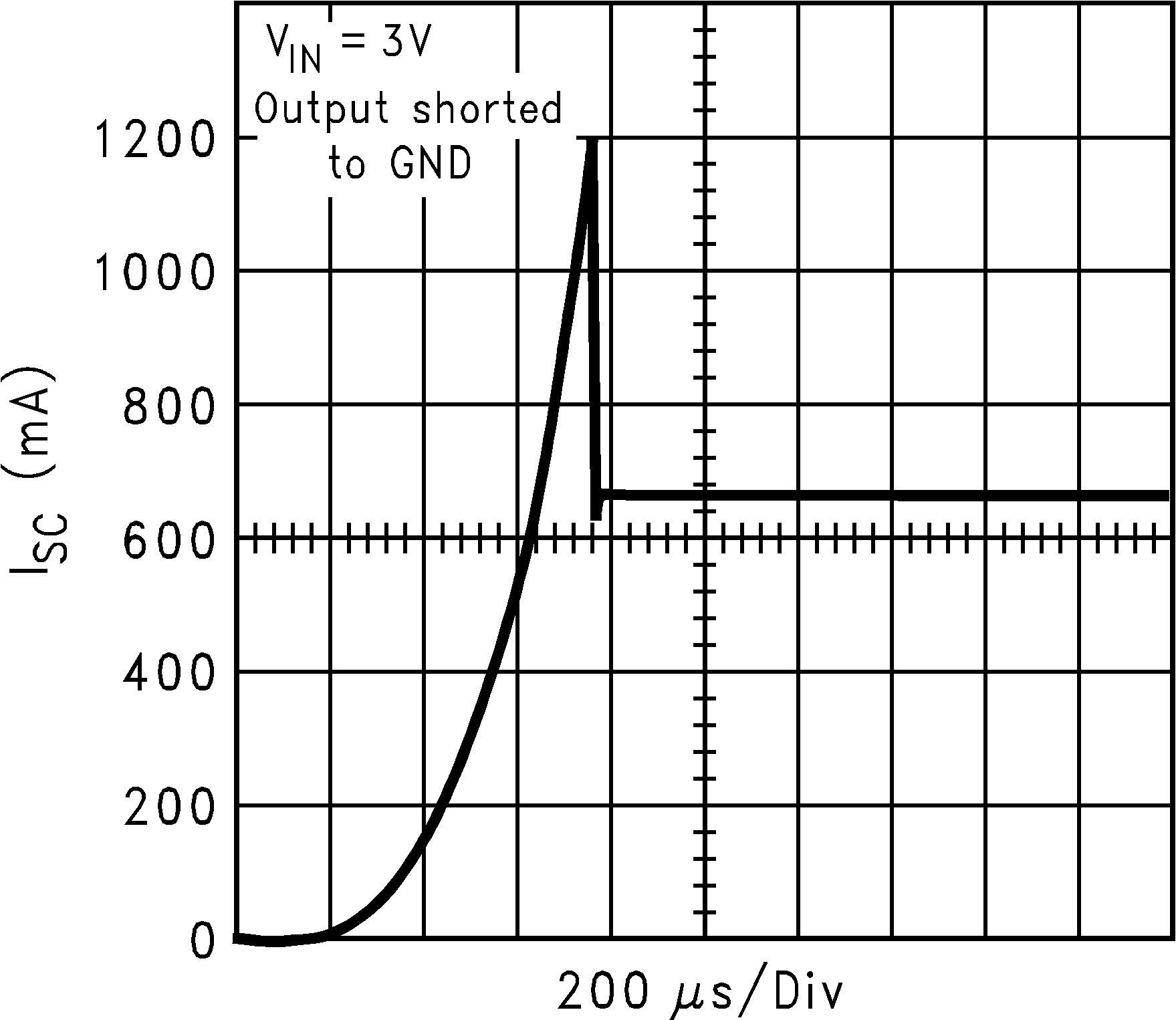
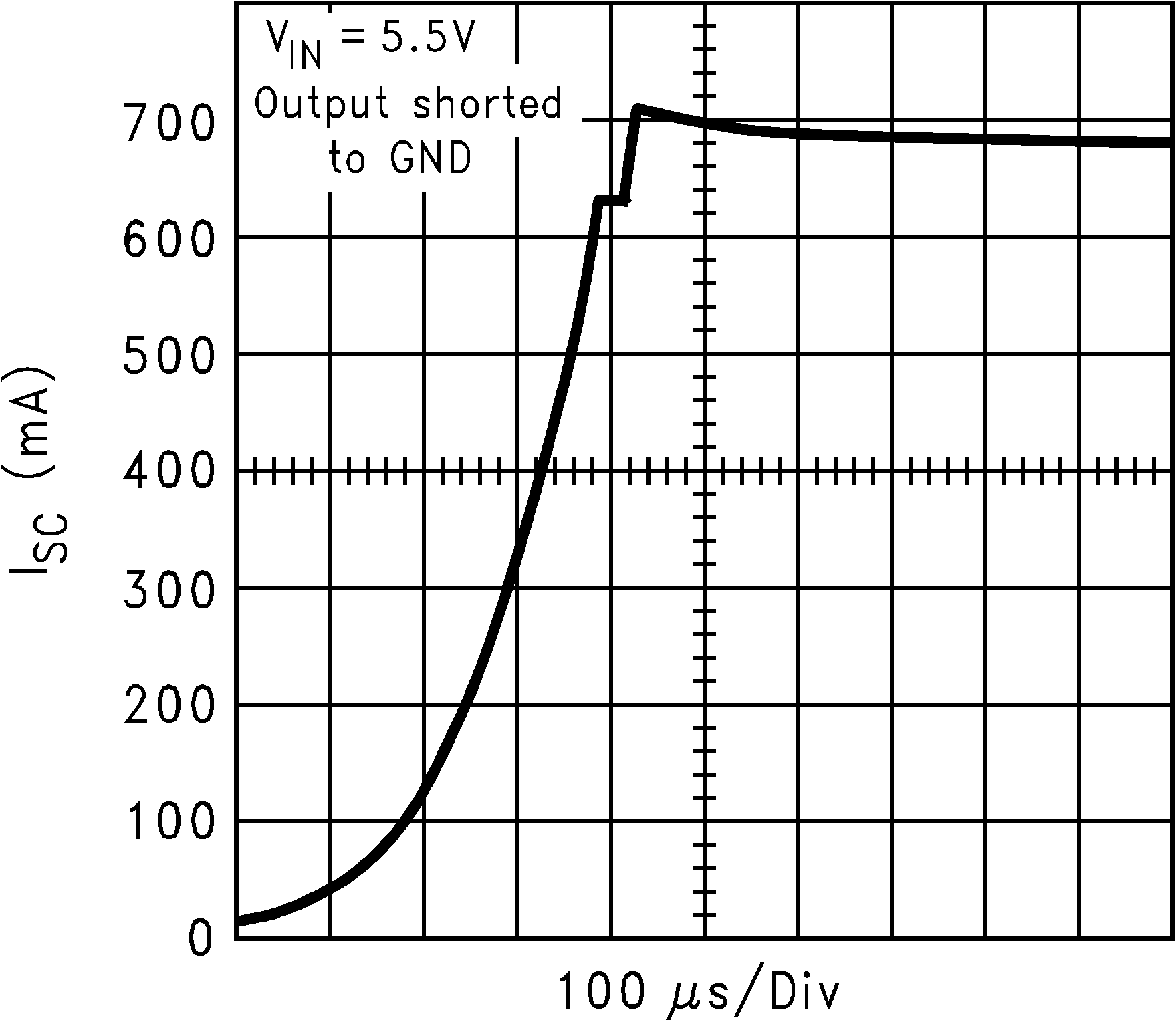
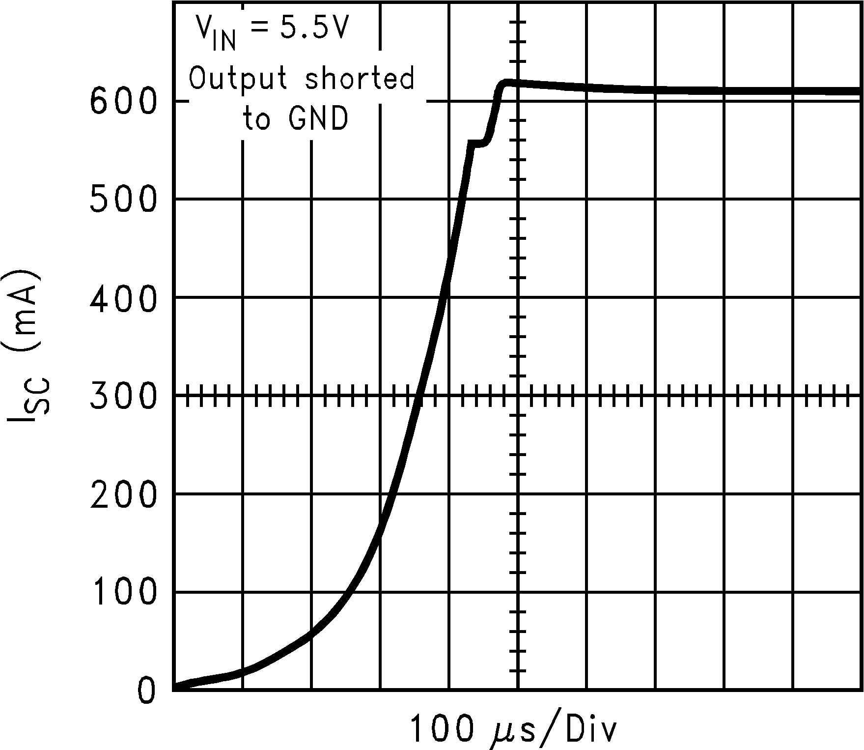
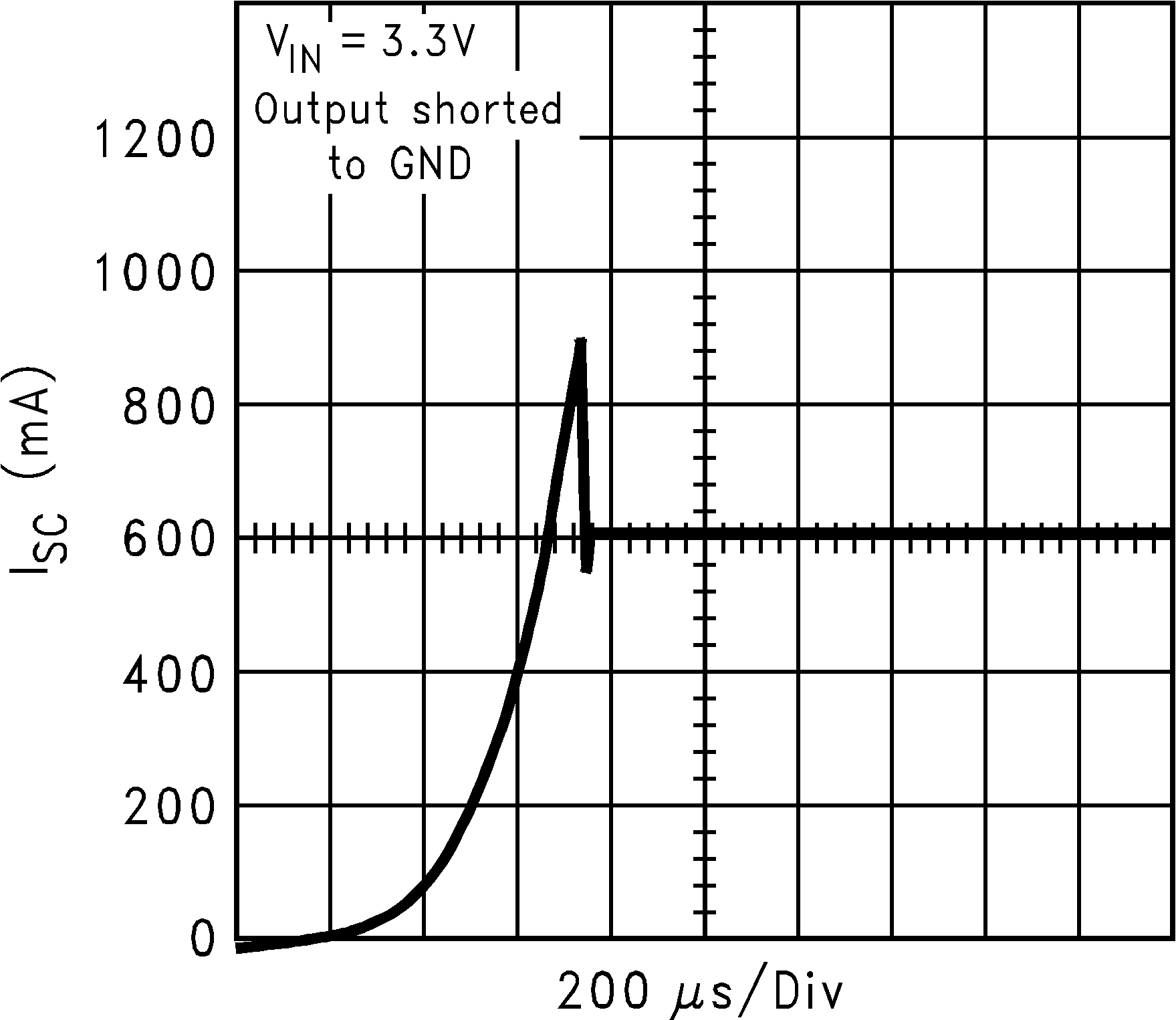
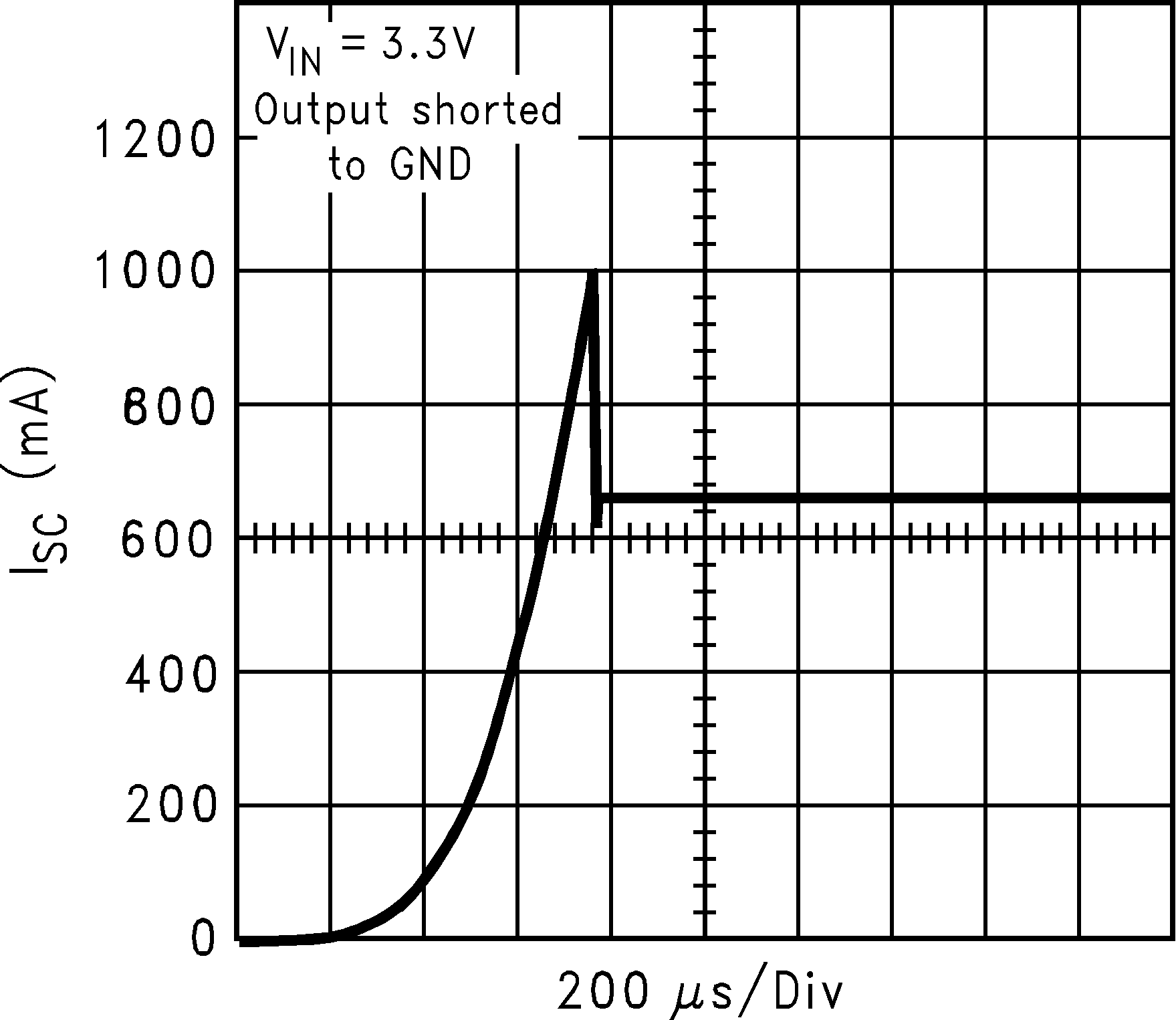
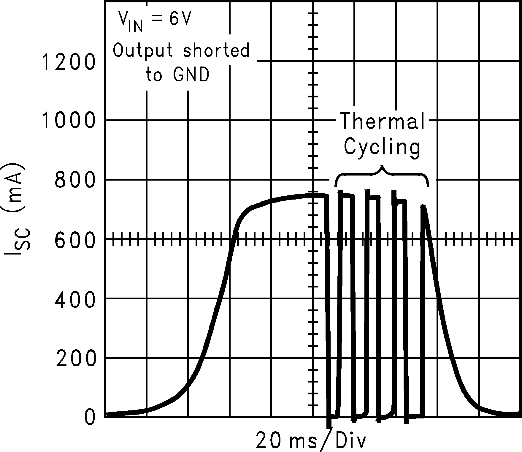
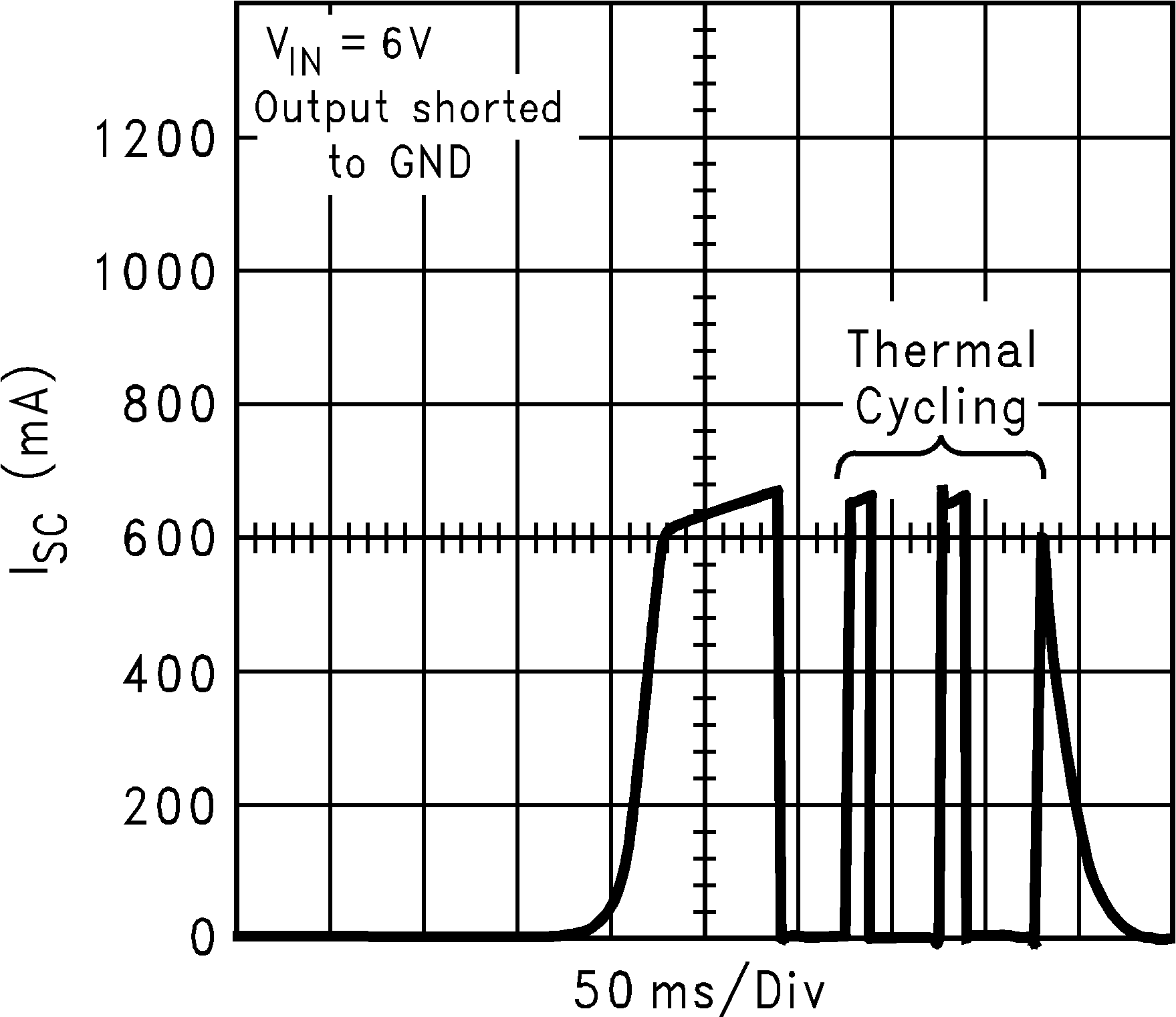
| ISC | Short circuit current limit | Output Grounded (Steady State) |
600 | mA | ||
| IOUT(PK) | Peak output current | VOUT ≥ VOUT(nom) – 5% | 300 | 550 | mA | |
| TON | Turnon time(6) | CBYPASS = 0.01 µF | 200 | µs | ||
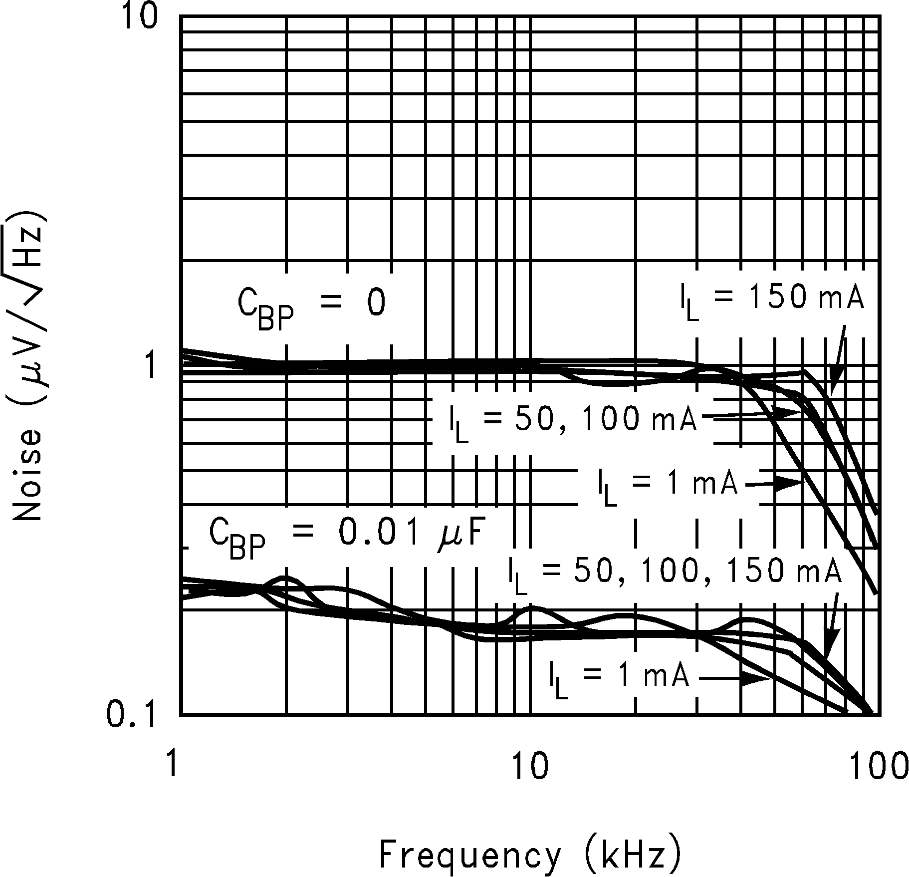
| en | Output noise voltage(7) | BW = 10 Hz to 100 kHz, COUT = 1 µF |
30 | µVRMS | ||
| Output noise density | CBP = 0 | 230 | nV/ √Hz | |||
| IEN | Maximum input current at EN | VEN = 0.4 V and VIN = 6 V | ±1 | nA | ||
| VIL | Maximum low-level input voltage at EN | VIN = 2.5 V to 6 V | 0.4 | V | ||
| VIH | Minimum high-level input voltage at EN | VIN = 2.5 V to 6 V | 1.4 | V | ||
| TSD | Thermal shutdown temperature | 160 | °C | |||
| Thermal shutdown hysteresis | 20 | °C | ||||
(1) All limits are verified. All electrical characteristics having room-temperature limits are tested during production with TA = 25°C or correlated using Statistical Quality Control (SQC) methods. All hot and cold limits are specified by correlating the electrical characteristics to process and temperature variations and applying statistical process control.
(2) The target output voltage, which is labeled VOUT(NOM), is the desired voltage option.
(3) TA = 25°C only.
(4) An increase in the load current results in a slight decrease in the output voltage and vice versa.
(5) Dropout voltage is the input-to-output voltage difference at which the output voltage is 100mV below its nominal value. This specification does not apply for input voltages below 2.5V.
(6) Turnon time is time measured between the enable input just exceeding VIH and the output voltage just reaching 95% of its nominal value.
(7) The output noise varies with output voltage option. The 30 µVRMS is measured with 2.5-V voltage option. To calculate an approximated output noise for other options, use the equation: (30µVRMS)(X)/2.5, where X is the voltage option value.
 Figure 1. Line Transient Input Test Signal
 Figure 2. PSRR Input Test Signal
6.6 Typical Performance Characteristics
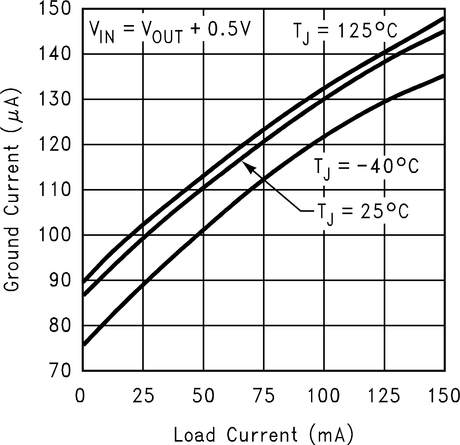
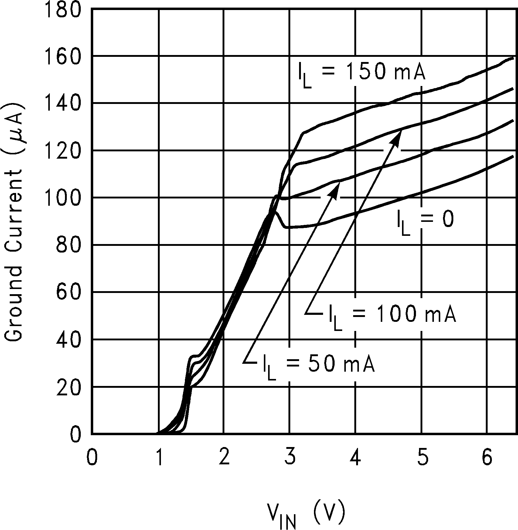
Unless otherwise specified, CIN = COUT = 1 µF ceramic, CBYPASS = 0.01 µF, VIN = VOUT + 0.2 V, TA = 25°C, EN pin is tied to VIN.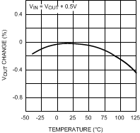
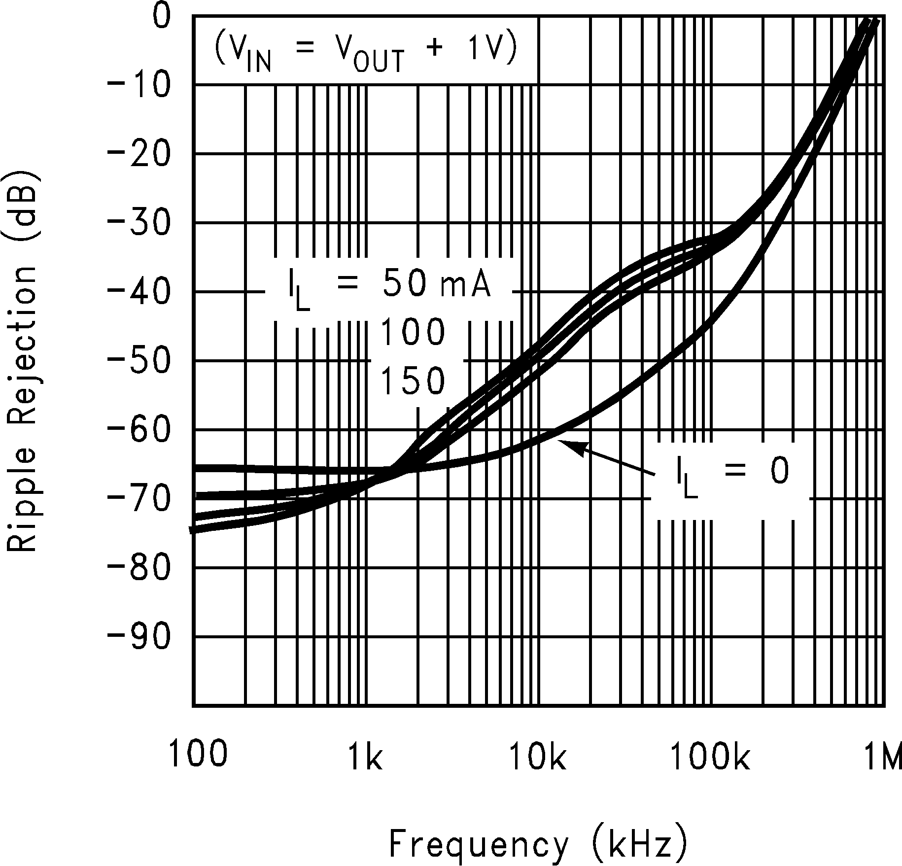
| VIN = VOUT + 1 V | ||
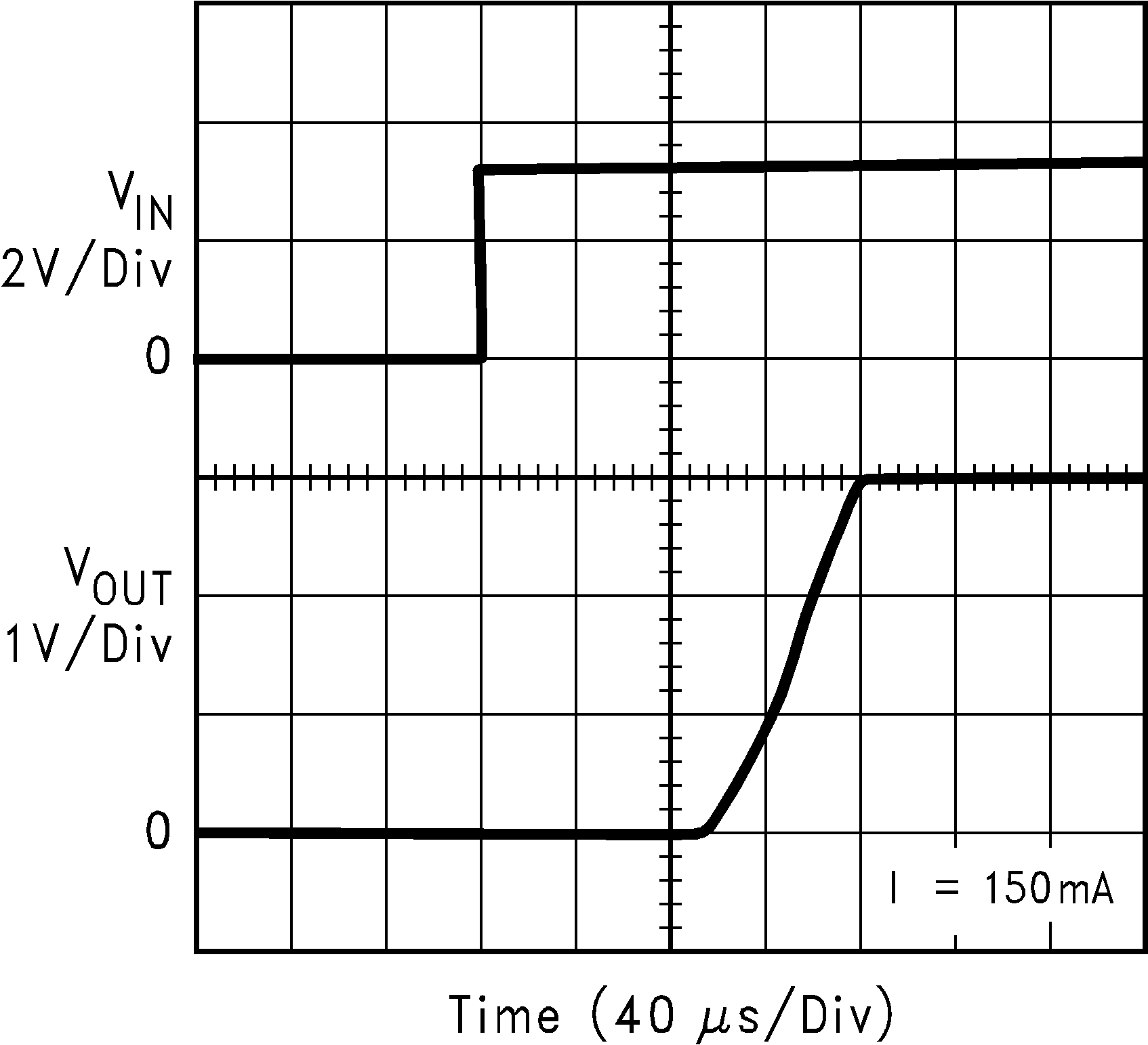
| VIN = VOUT + 0.2 V | ||
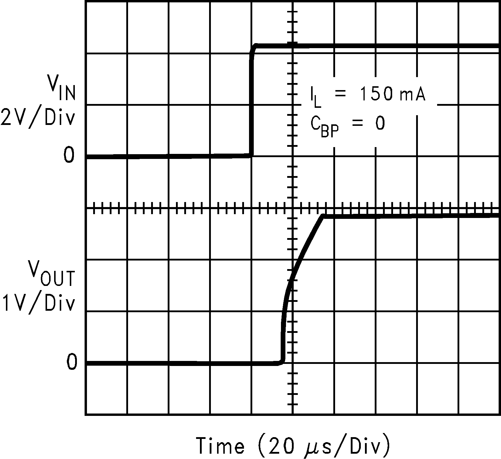
| VIN = 4.2 V | ||
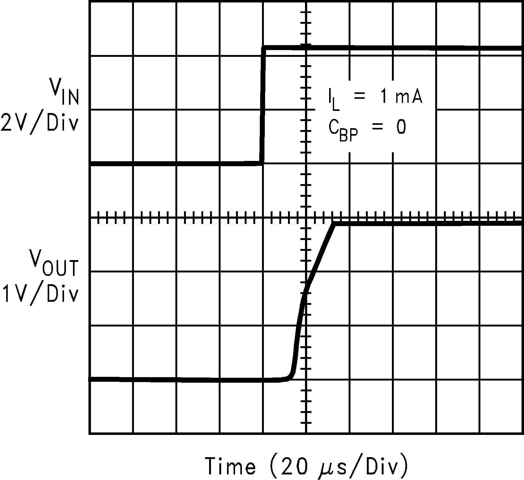
| VIN = 4.2 V | ||
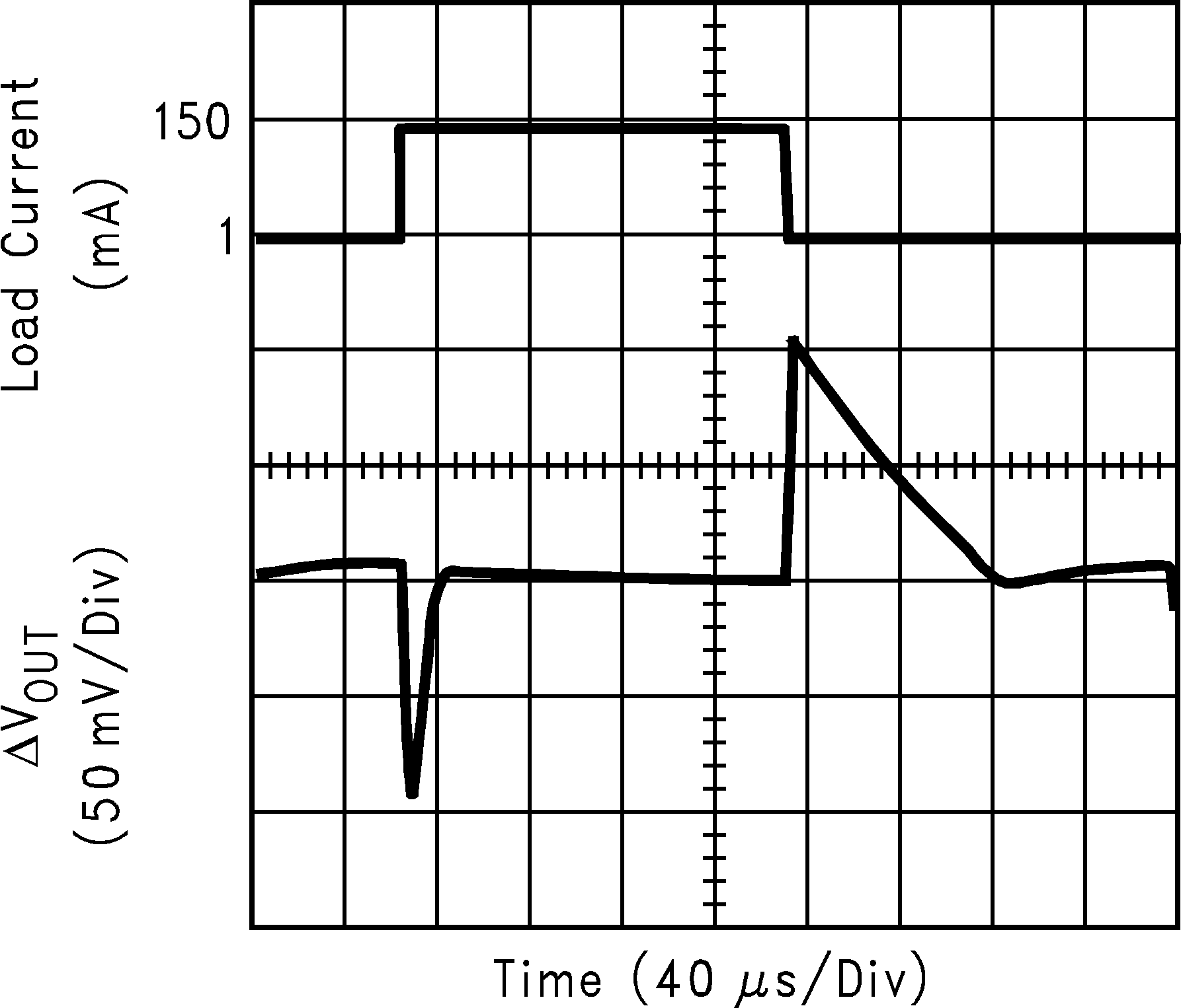
| VIN = 4.2 V | ||
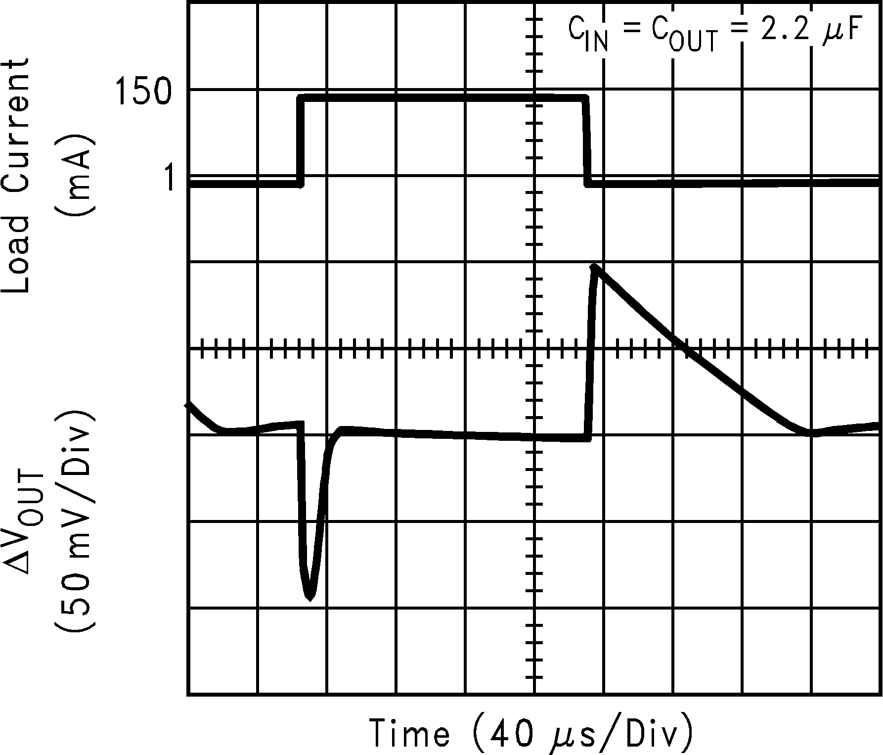
| VIN = 4.2 V | ||
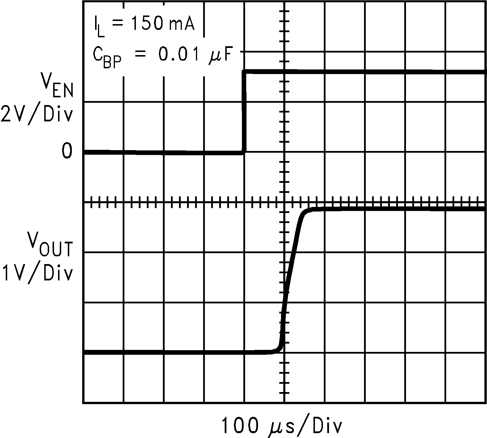
| VIN = VOUT + 0.2 V | ||
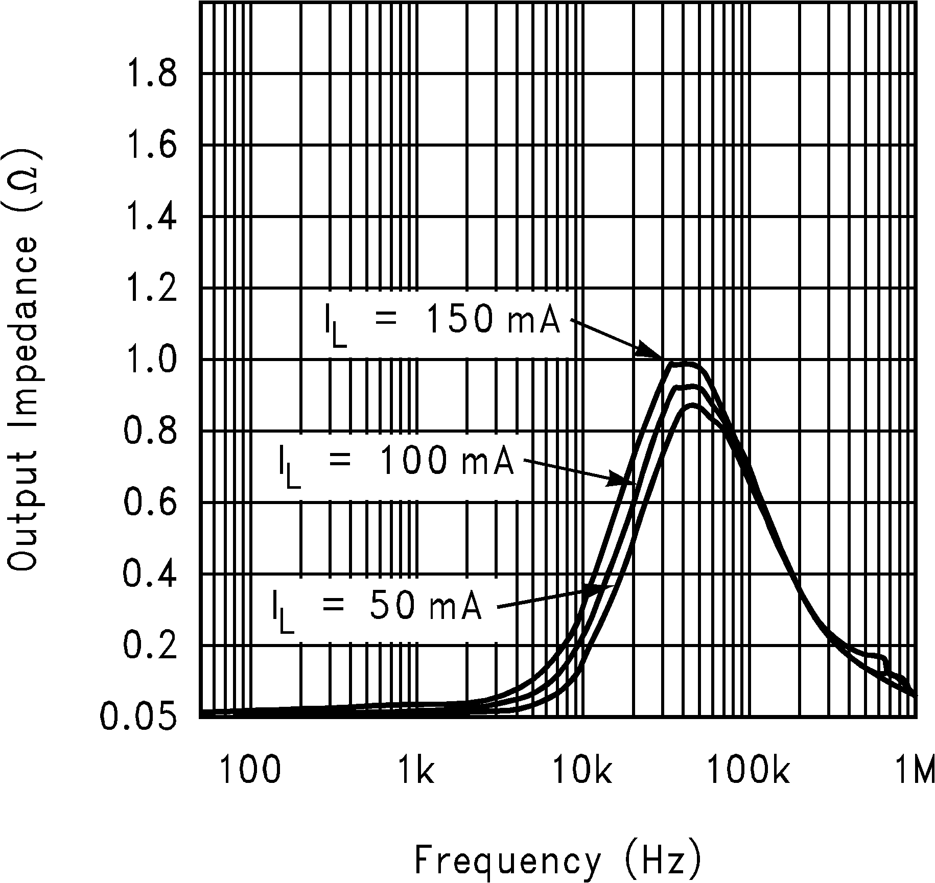
| VIN = 4.2 V | ||
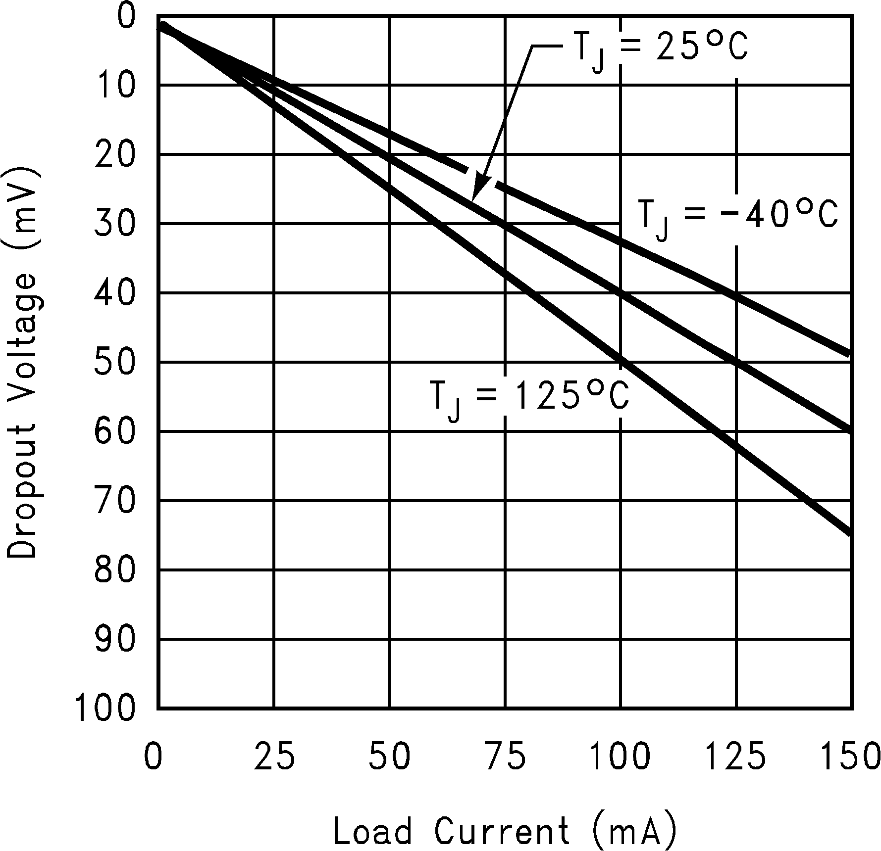
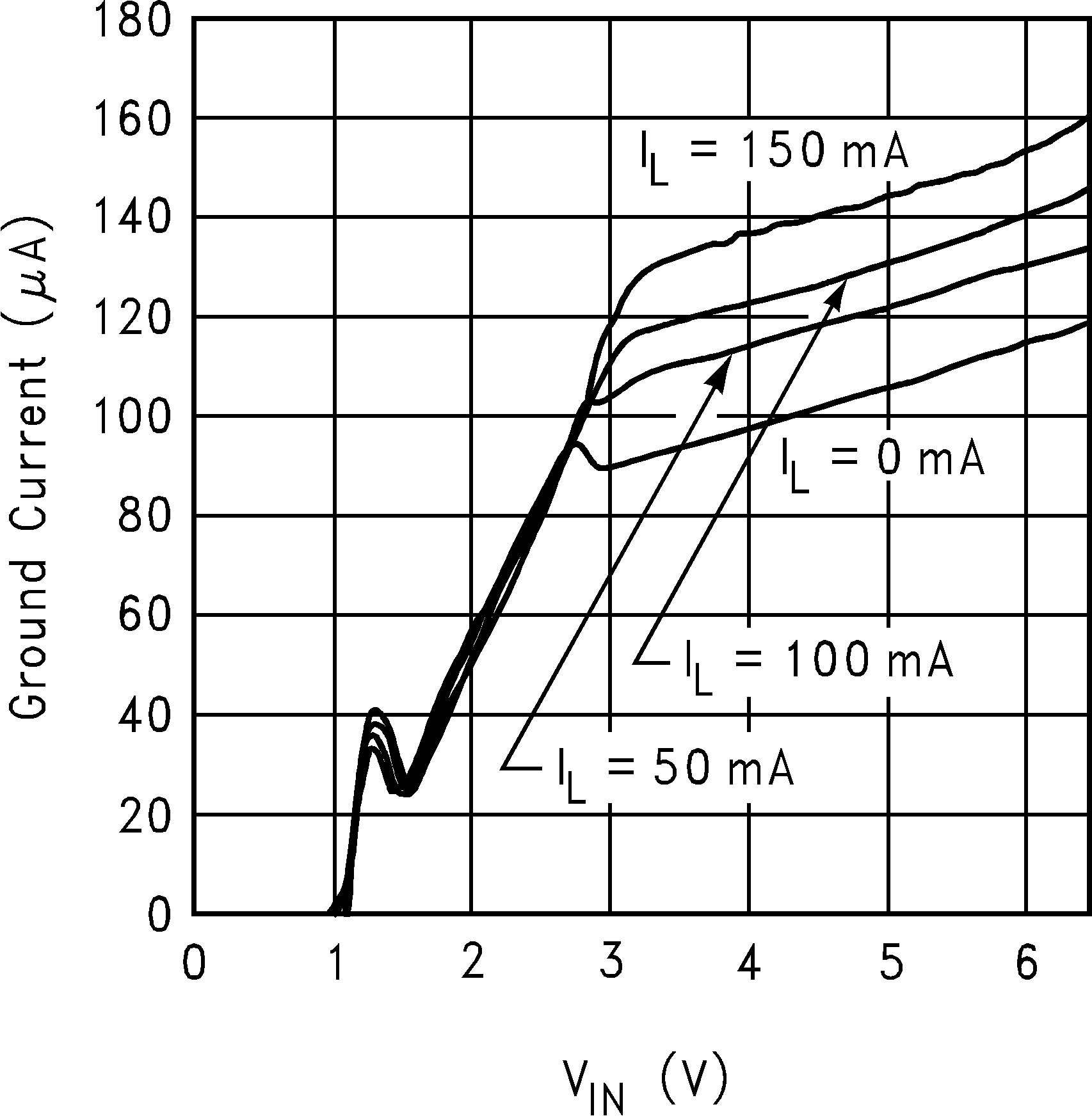
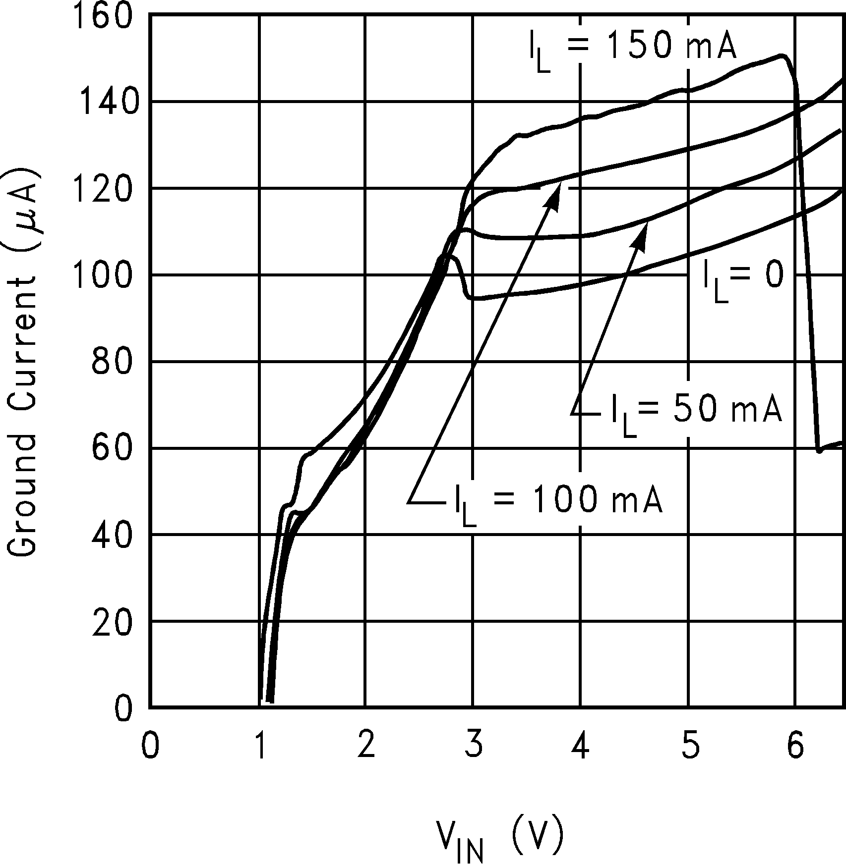
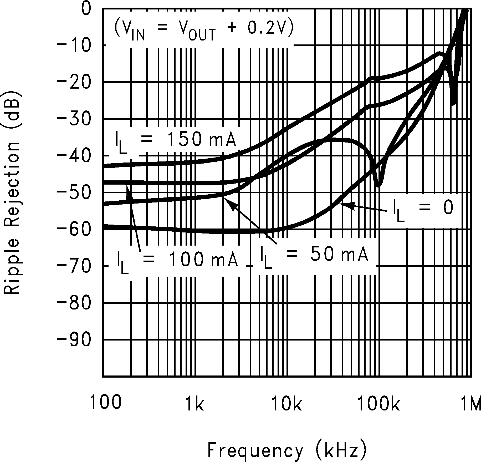
| VIN = VOUT + 0.2 V | ||
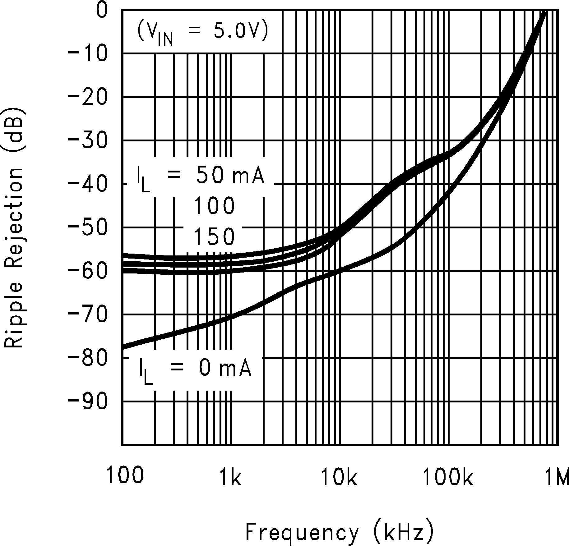
| VIN = 5 V | ||
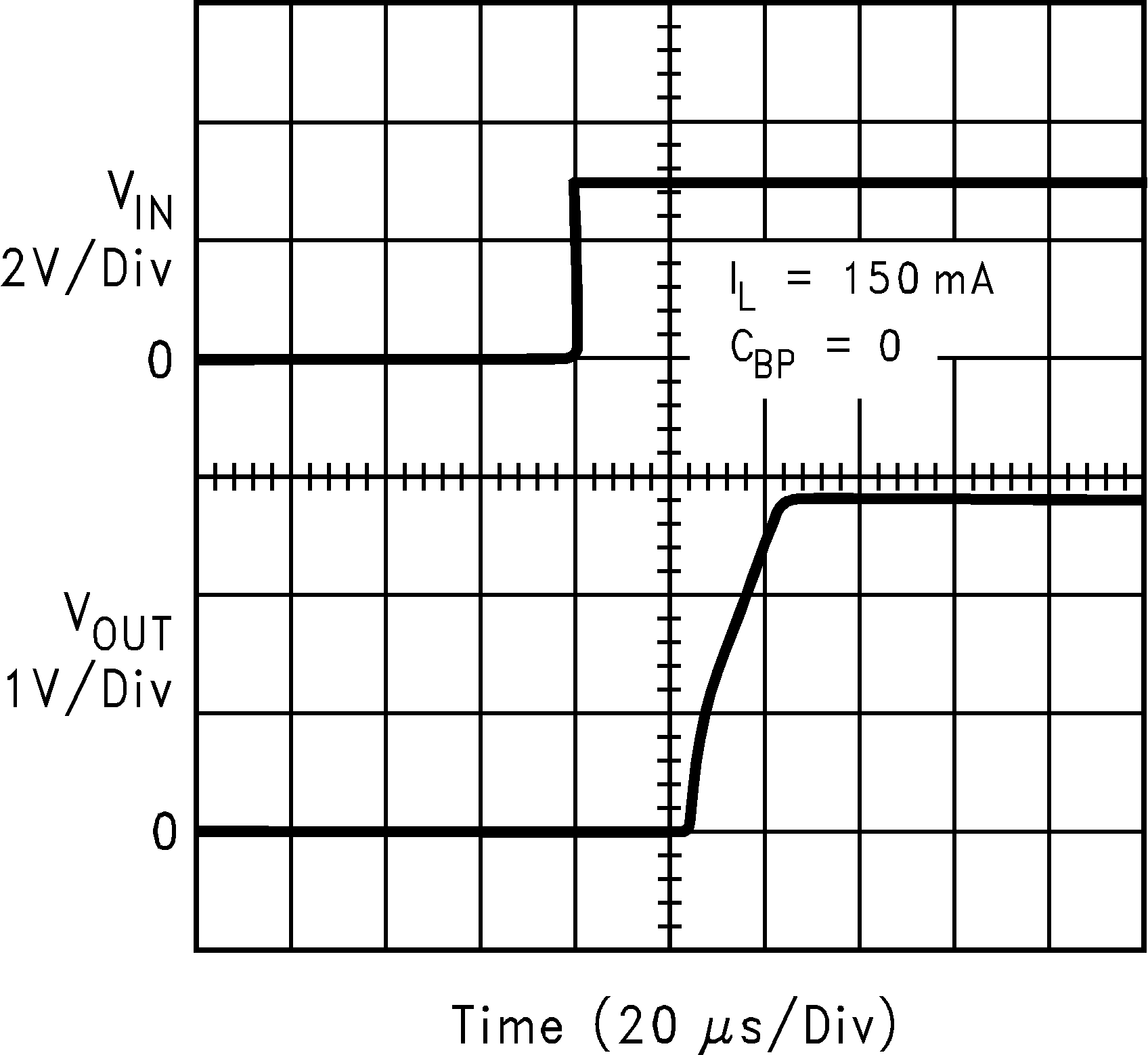
| VIN = VOUT + 0.2 V | ||
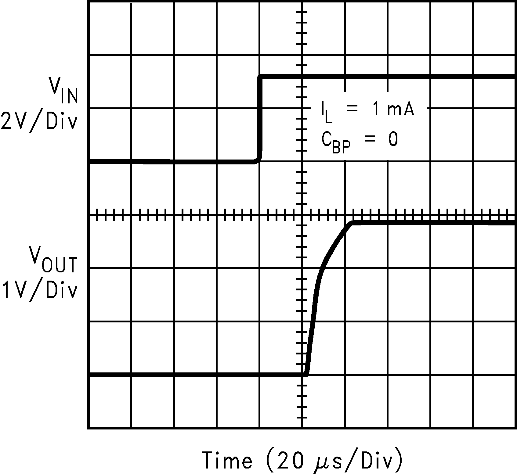
| VIN = VOUT + 0.2 V | ||
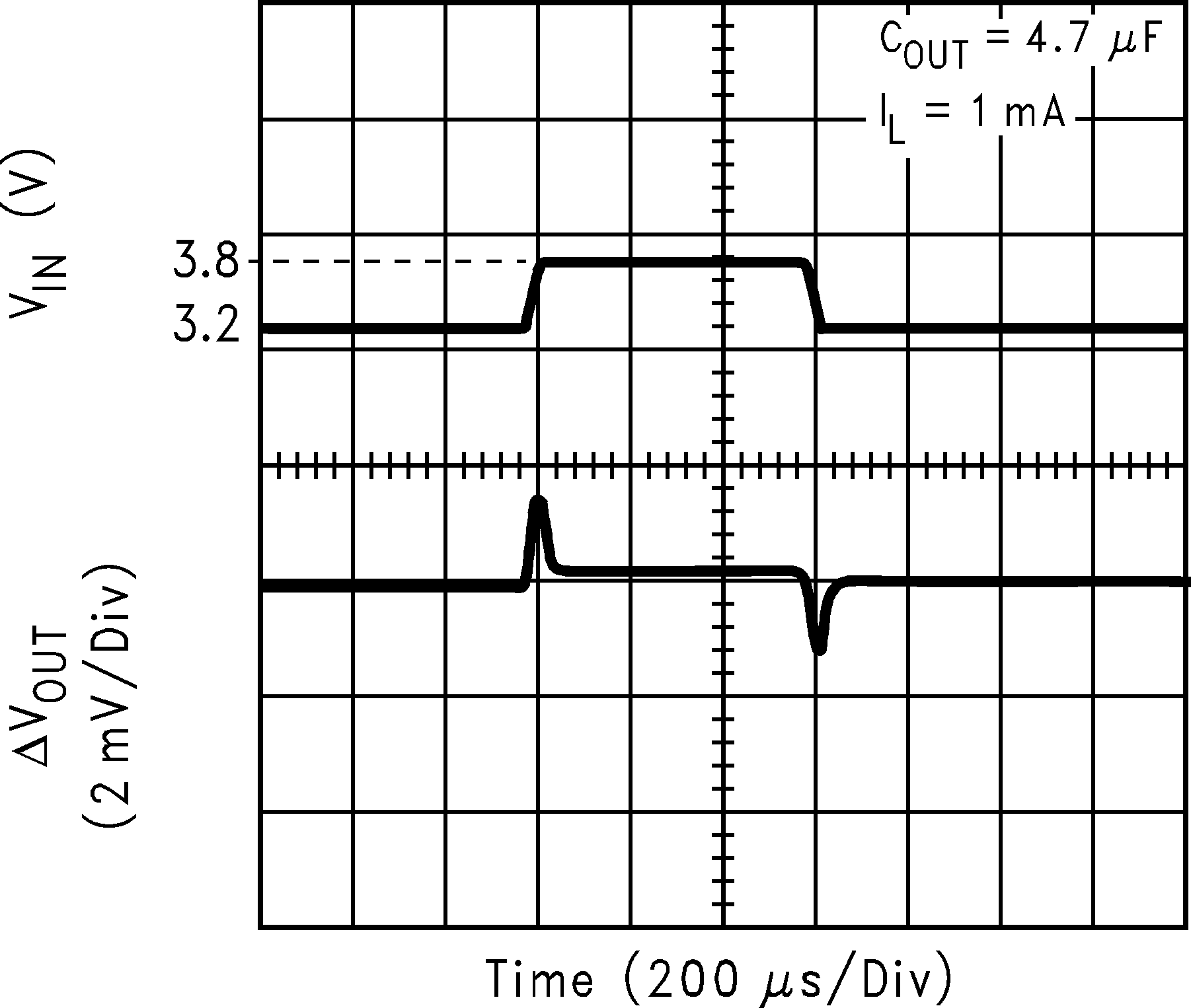
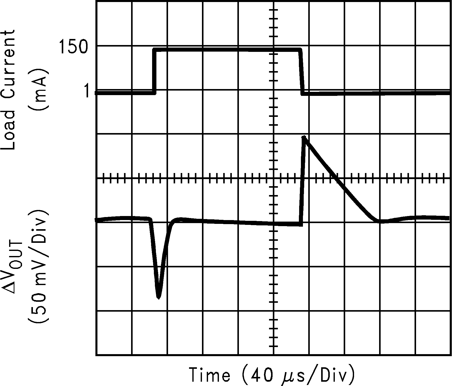
| VIN = 3.2 V | ||
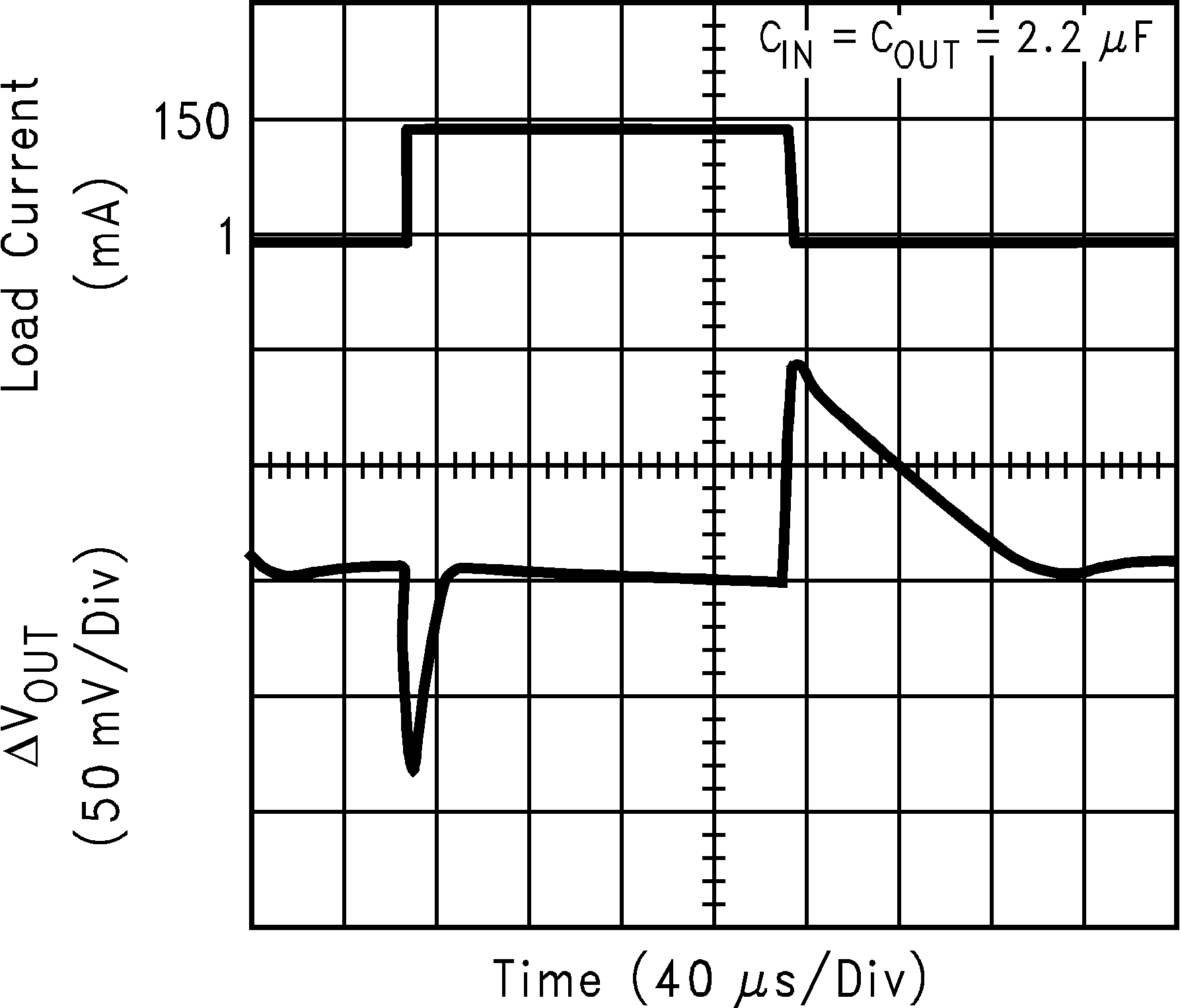
| VIN = 3.2 V | ||
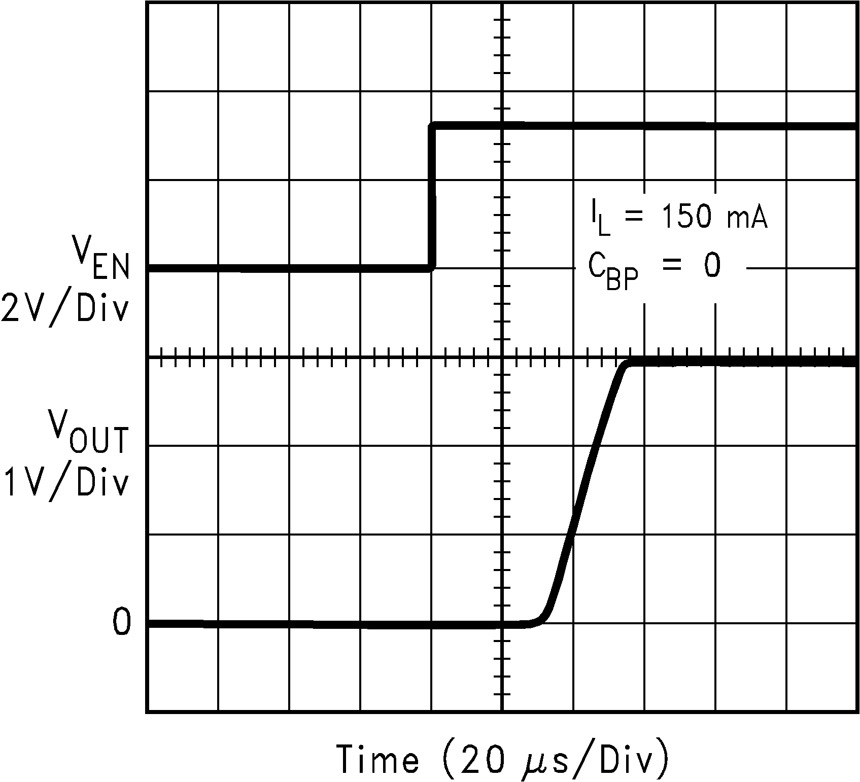
| VIN = VOUT + 0.2 V | ||
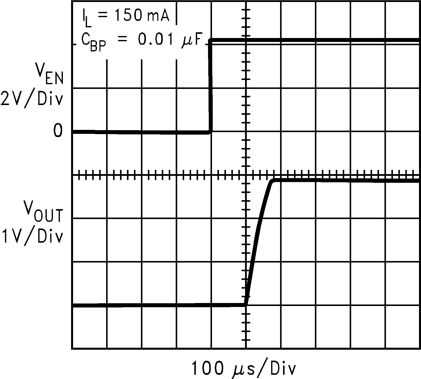
| VIN = 4.2 V | ||
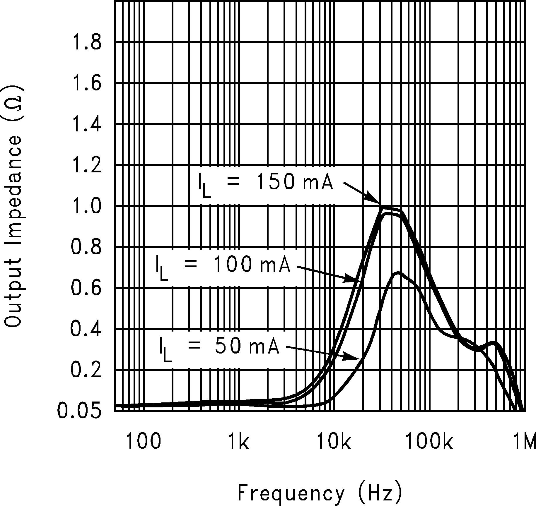
| VIN = VOUT + 0.2 V | ||