SNVS500C July 2007 – November 2016 LP5524
PRODUCTION DATA.
- 1 Features
- 2 Applications
- 3 Description
- 4 Revision History
- 5 Pin Configuration and Functions
- 6 Specifications
- 7 Detailed Description
- 8 Application and Implementation
- 9 Power Supply Recommendations
- 10Layout
- 11Device and Documentation Support
- 12Mechanical, Packaging, and Orderable Information
Package Options
Mechanical Data (Package|Pins)
- YFQ|9
Thermal pad, mechanical data (Package|Pins)
Orderable Information
7 Detailed Description
7.1 Overview
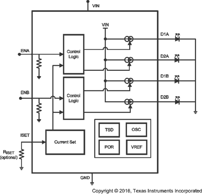
The LP5524 is an easy-to-use high side current source capable of driving 4 indicator LEDs with up to 25 mA per LED. The device operates over the 2.7-V to 5.5-V input voltage range. The output current is user-programmable via the optional external ISET resistor.
7.2 Functional Block Diagram

7.3 Feature Description
7.3.1 LED
Forward voltage of LED must be less than minimum input voltage minus minimum headroom voltage (VHR). For example with 2.7-V input voltage and 20-mA LED current the maximum LED forward voltage is 2.7 V – 100 mV = 2.6 V.
7.3.2 LED Headroom Voltage
A single current source is connected internally between VIN and DX outputs (D1A, D2A, D1B and D2B). The voltage across the current source, (VIN – VDX), is referred to as headroom voltage (VHR). The current source requires a sufficient amount of headroom voltage to be present across it in order to regulate properly.
Figure 4 shows how output current of the LP5524 varies with respect to headroom voltage. On the flat part of the graph, the current is regulated properly as there is sufficient headroom voltage for regulation. On the sloping part of the graph the headroom voltage is too small, the current source is squeezed, and the current drive capability is limited. Thus, operating the LP5524 with insufficient headroom voltage across the current source must be avoided.
7.3.3 LED Outputs
If more than 25 mA of output current is required LED outputs can be connected parallel. Connecting LED outputs of different group parallel generates a simply two stage brightness control. With IDX set to 25 mA, enabling one group sets the LED current to 25 mA. Enabling second bank increases the LED current to 50 mA. Unused LED outputs can be left floating or tied to VIN.
7.3.4 PWM Brightness Control
The brightness of LEDs can be linearly varied from zero up to the maximum programmed current level by applying a pulse–width–modulated signal to the ENx pin of the LP5524. The following procedures illustrate how to program the LED drive current and adjust the output current level using a PWM signal.
- Determine the maximum desired LED current. Use Equation 1 to calculate RISET.
- Brightness control can be implemented by pulsing a signal at the ENx pin. LED brightness is proportional to the duty cycle (D) of the PWM signal.
For linear brightness control over the full duty cycle adjustment range, the LP5524 uses a special turnoff time delay to compensate the turn–on time of the device.
If the PWM frequency is much less than 100 Hz, flicker may be seen in the LEDs. For the LP5524, zero duty cycle turns off the LEDs and a 50% duty cycle results in an average IDX being half of the programmed LED current. For example, if RISET is set to program LED current to 15 mA, a 50% duty cycle results in an average IDX of 7.5mA.
7.4 Device Functional Modes
7.4.1 Enable Mode
The LP5524 has four constant current LED outputs, which are split into two independently controlled banks. Each bank has its own enable input. ENA is used to control bank A and ENB is used to control bank B. Both enables are active high and have internal pulldown resistors. When both enables are low part is in low power standby mode. Driving either enable high activates the device and corresponding LED outputs.
7.4.2 ISET Pin
An external resistor (RISET) connected to ISET pin sets the output current of all the LEDs. The internal current mirror sets the LEDs output current with a 416:1 ratio to the current through RISET. Equation 1 approximates the LED current:
The use of RISET is optional. If RISET is not used the ISET pin can be left floating or connected to VIN. In these cases LED current is set to default current.