SNVS500C July 2007 – November 2016 LP5524
PRODUCTION DATA.
- 1 Features
- 2 Applications
- 3 Description
- 4 Revision History
- 5 Pin Configuration and Functions
- 6 Specifications
- 7 Detailed Description
- 8 Application and Implementation
- 9 Power Supply Recommendations
- 10Layout
- 11Device and Documentation Support
- 12Mechanical, Packaging, and Orderable Information
Package Options
Mechanical Data (Package|Pins)
- YFQ|9
Thermal pad, mechanical data (Package|Pins)
Orderable Information
6 Specifications
6.1 Absolute Maximum Ratings
over operating free-air temperature range (unless otherwise noted)(1)(2)(3)(5)| MIN | MAX | UNIT | ||
|---|---|---|---|---|
| V (VIN, DX, ISET) | –0.3 | 6 | V | |
| Voltage on logic pins (ENA, ENB) | –0.3 | 6 | V | |
| Continuous power dissipation(4) | Internally limited | |||
| Junction temperature, TJ-MAX | 125 | °C | ||
| Storage temperature, Tstg | –65 | 150 | °C | |
(1) Stresses beyond those listed under Absolute Maximum Ratings may cause permanent damage to the device. These are stress ratings only, which do not imply functional operation of the device at these or any other conditions beyond those indicated under Recommended Operating Conditions. Exposure to absolute-maximum-rated conditions for extended periods may affect device reliability.
(2) If Military/Aerospace specified devices are required, contact the Texas Instruments Sales Office/ Distributors for availability and specifications.
(3) All voltages are with respect to the potential at the GND pin.
(4) Internal thermal shutdown circuitry protects the device from permanent damage. Thermal shutdown engages at TJ=160°C (typical) and disengages at TJ=140°C (typical).
(5) For detailed soldering specifications and information, refer to AN-1112 DSBGA Wafer Level Chip Scale Package and Absolute Maximum Ratings for Soldering.
6.2 ESD Ratings
| VALUE | UNIT | |||
|---|---|---|---|---|
| V(ESD) | Electrostatic discharge | Human-body model (HBM), per ANSI/ESDA/JEDEC JS-001(1) | ±2000 | V |
(1) JEDEC document JEP155 states that 500-V HBM allows safe manufacturing with a standard ESD control process.
6.3 Recommended Operating Conditions
over operating free-air temperature range (unless otherwise noted)| MIN | MAX | UNIT | ||
|---|---|---|---|---|
| Voltage on power pin (VIN) | 2.7 | 5.5 | V | |
| Junction temperature, TJ | –40 | 125 | °C | |
| Ambient temperature, TA(1) | –40 | 85 | °C | |
(1) In applications where high power dissipation and/or poor package thermal resistance is present, the maximum ambient temperature may have to be derated. Maximum ambient temperature (TA-MAX) is dependent on the maximum operating junction temperature (TJ-MAX-OP = 125°C), the maximum power dissipation of the device in the application (PD-MAX), and the junction-to ambient thermal resistance of the part/package in the application (RθJA), as given by the following equation: TA-MAX = TJ-MAX-OP – (RθJA × PD-MAX).
6.4 Thermal Information
| THERMAL METRIC(1) | LP5524 | UNIT | |
|---|---|---|---|
| YFQ (DSBGA) | |||
| 9 PINS | |||
| RθJA | Junction-to-ambient thermal resistance(2) | 101.9 | °C/W |
| RθJC(top) | Junction-to-case (top) thermal resistance | 0.9 | °C/W |
| RθJB | Junction-to-board thermal resistance | 22.7 | °C/W |
| ψJT | Junction-to-top characterization parameter | 0.4 | °C/W |
| ψJB | Junction-to-board characterization parameter | 22.7 | °C/W |
(1) For more information about traditional and new thermal metrics, see the Semiconductor and IC Package Thermal Metrics application report.
(2) Junction-to-ambient thermal resistance is highly application and board-layout dependent. In applications where high maximum power dissipation exists, special care must be paid to thermal dissipation issues in board design.
6.5 Electrical Characteristics
Unless otherwise noted, specifications apply to the Functional Block Diagram with: VIN = 3.6 V, RISET = 32.4 kΩ, CIN = 100 nF, TJ = 25°C.(1)(2)| PARAMETER | TEST CONDITIONS | MIN | TYP | MAX | UNIT | |
|---|---|---|---|---|---|---|
| IVIN | Shutdown supply current | ENA = ENB = 0 V | 0.2 | µA | ||
| ENA = ENB = 0V, TJ = –40°C to 85°C | 1 | |||||
| Active mode supply current | ENA = ENB = H, ISET = open | 170 | µA | |||
| ENA = ENB = H, ISET = open TJ = –40°C to 85°C |
210 | |||||
| IDX | Recommended LED current | 3 | 25 | mA | ||
| IOUT | LED output current accuracy | IDX = 5 mA, VDX = VIN – 0.2V ISET = open |
0.5% | |||
| IDX = 5 mA, VDX = VIN – 0.2V ISET = open, TJ = –40°C to 85°C |
5% | |||||
| IDX = 15.9 mA, VDX = VIN – 0.2 V | 0.5% | |||||
| IDX = 15.9 mA, VDX = VIN – 0.2 V TJ = –40°C to 85°C |
4% | |||||
| IMATCH | LED current matching(3) | IDX = 15.9 mA | 0.4% | |||
| IDX = 15.9 mA, TJ = –40°C to 85°C | 2.5% | |||||
| ΔIDX%/ΔVIN | Line regulation | 1 | %/V | |||
| ΔIDX%/ΔVDX | Load regulation | VDX < VIN – 0.2V | 0.4 | %/V | ||
| VHR | Minimum headroom voltage (VIN – VDX)(4) |
IDX set to 5 mA | 10 | mV | ||
| IDX set to 15 mA | 30 | mV | ||||
| IDX set to 15 mA, TJ = –40°C to 85°C | 75 | |||||
| IMIRROR | External RISET to LED current mirroring ratio |
1:416 | ||||
| VISET | ISET reference voltage | 1.237 | V | |||
| IISET | TJ = –40°C to 85°C | 2.5 | 62.5 | µA | ||
| tPWM MIN | Recommended minimum ON time for PWM signal |
33 | μs | |||
| VIL | Logic input low level | TJ = –40°C to 85°C | 0.4 | V | ||
| VIH | Logic input high level | TJ = –40°C to 85°C | 1.2 | V | ||
| IIN | CTRL input current | ENA / ENB = 1.2 V | 1.2 | µA | ||
| ENA / ENB = 1.2 V, TJ = –40°C to 85°C | 1.9 | |||||
| tSD | Shutdown delay time | Delay from ENA and ENB = low to IDX = 0.1 × IDX nom |
20 | 25 | µs | |
(1) All voltages are with respect to the potential at the GND pin.
(2) Minimum (MIN) and maximum (MAX) limits are specified by design, test, or statistical analysis. Typical (TYP) numbers represent the most likely norm.
(3) Matching is the maximum difference from the average.
(4) The current source is connected internally between VIN an VDX. The voltage across the current source, (VIN – VDX), is referred to a headroom voltage (VHR). Minimum headroom voltage is defined as the VHR voltage when the LED current has dropped 20% from the value measured at VDX = VIN – 1 V.
6.6 LED Driver Typical Characteristics
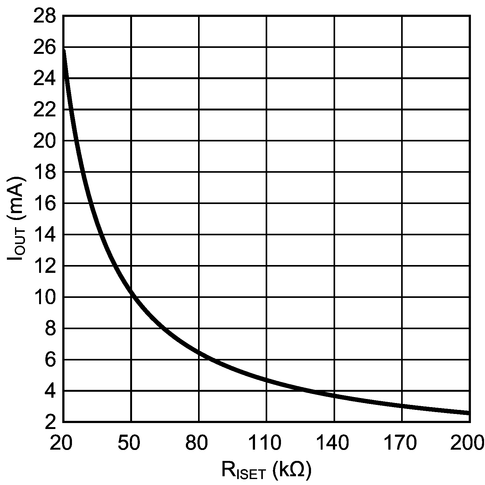
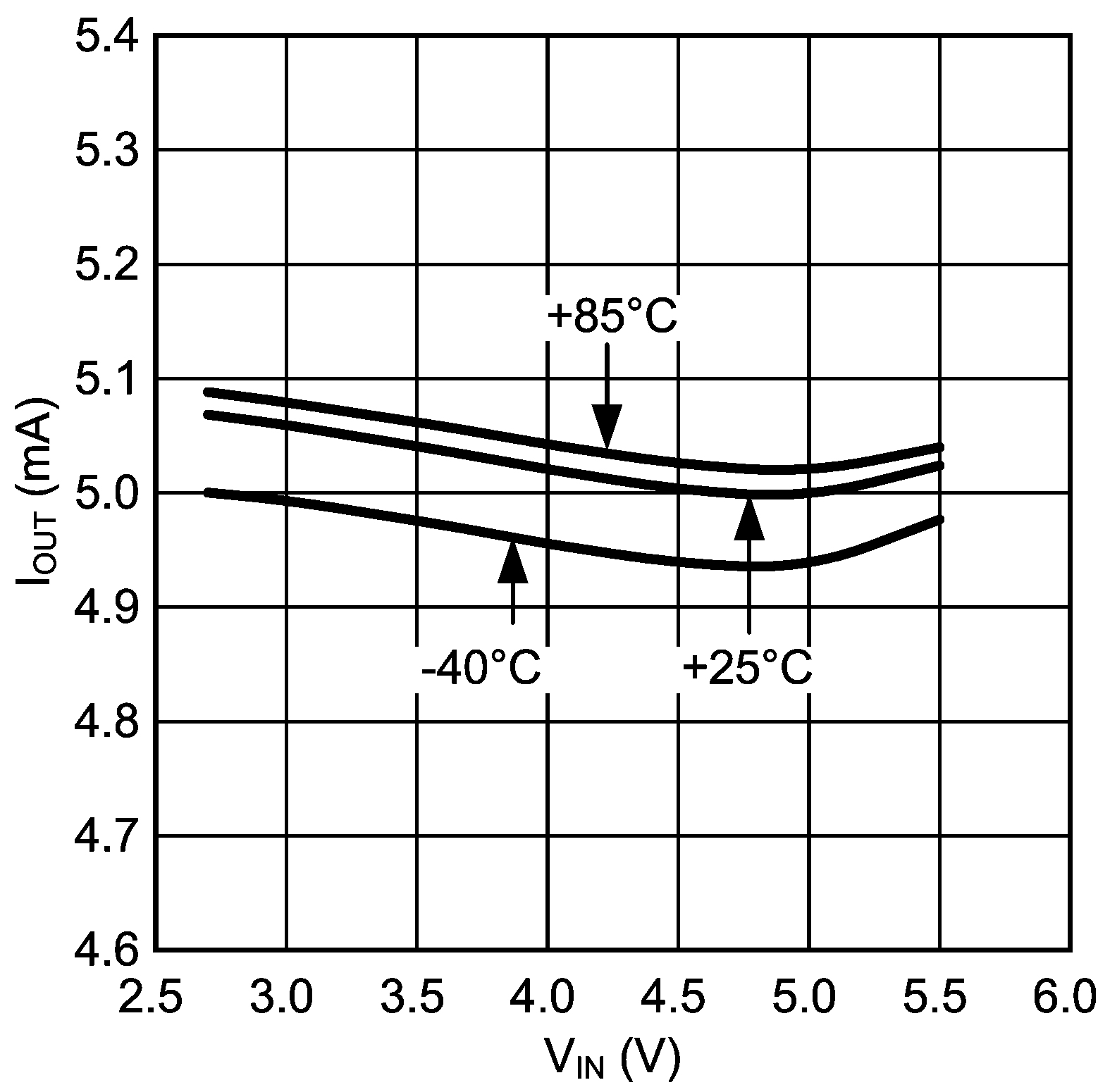
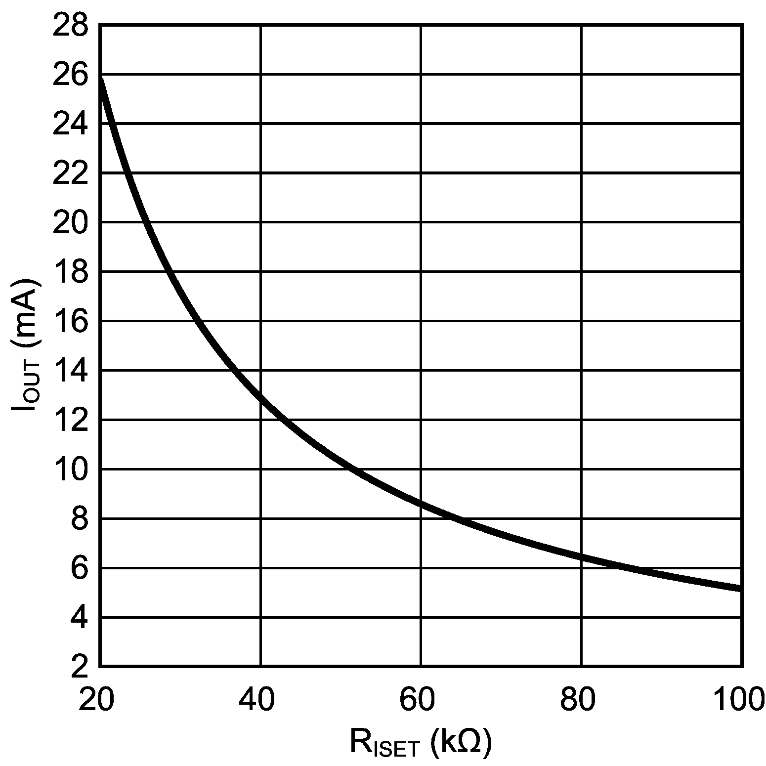
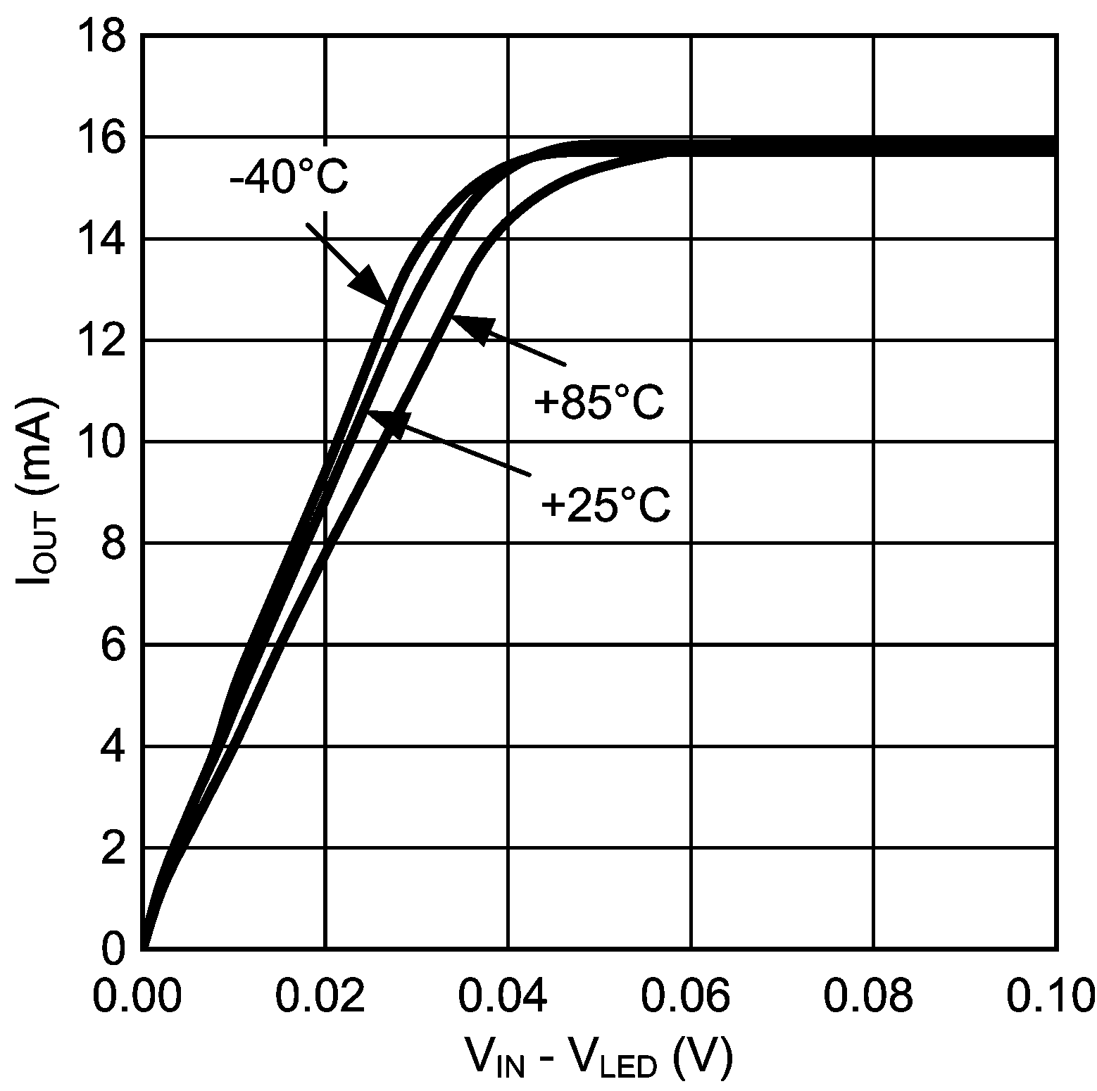
TJ = 25°C. Unless otherwise noted, typical performance characteristics apply to the Functional Block Diagram with VIN = 3.6 V, RISET = 32.4 kΩ, CIN = 100 nF.


