SLVSGD5 July 2021 LP5890
PRODUCTION DATA
- 1 Features
- 2 Applications
- 3 Description
- 4 Revision History
- 5 Description (continued)
- 6 Pin Configuration and Functions
- 7 Specifications
-
8 Detailed Description
- 8.1 Overview
- 8.2 Functional Block Diagram
- 8.3
Feature Description
- 8.3.1 Independent and Stackable Mode
- 8.3.2 Current Setting
- 8.3.3 Frequency Multiplier
- 8.3.4 Line Transitioning Sequence
- 8.3.5 Protections and Diagnostics
- 8.4 Device Functional Modes
- 8.5 Continuous Clock Series Interface
- 8.6 PWM Grayscale Control
- 8.7 Register Maps
- 9 Application and Implementation
- 10Power Supply Recommendations
- 11Layout
- 12Device and Documentation Support
- 13Mechanical, Packaging, and Orderable Information
Package Options
Mechanical Data (Package|Pins)
Thermal pad, mechanical data (Package|Pins)
Orderable Information
9.2.1.3 Internal GCLK Frequency
The internal GCLK frequency is configured by the Frequency Multiplier (FREQ_MUL) and is determined by the PWM resolution. The GCLK frequency can be calculated by the below equations:
Equation 3. 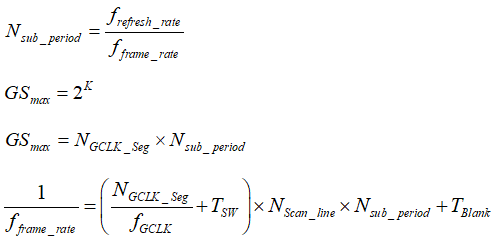
where
- frefresh_rate means the refresh rate
- fframe_rate means the frame rate
- K means the PWM resolution
- Nsub_period means the sub-period numbers within one frame
- NGCLK_seg means the GCLK number per segment (line switch time excluded)
- fGCLK means GCLK frequency
- TSW means line switching time
- Nscan_line means the scan line number
- Tblank means the blank time in one frame, equals to 0 in ideal configuration
- GSmax means the maximum grayscale that the device can output in one frame
Table 9-2 gives the values based on the system configuration and equation.
Table 9-2 LP5890 Design Parameters for GCLK Frequency Calculation
| DESIGN PARAMETER | EXAMPLE VALUE |
|---|---|
| Nsub_period | 32 |
| Nscan_line | 30 |
| TSW | 1.5 µs |
| Tblank | 0 |
| NGCLK_seg | 512 |
| GSmax | 16383 |
| fGCLK | 71.3 MHz |
Considering SCLK frequency and FREQ_MUL, the SCLK can be 27.7 MHz and FREQ_MUL can be 0010b. So the GCLK will be 83.1 MHz.