SLVSGD5 July 2021 LP5890
PRODUCTION DATA
- 1 Features
- 2 Applications
- 3 Description
- 4 Revision History
- 5 Description (continued)
- 6 Pin Configuration and Functions
- 7 Specifications
-
8 Detailed Description
- 8.1 Overview
- 8.2 Functional Block Diagram
- 8.3
Feature Description
- 8.3.1 Independent and Stackable Mode
- 8.3.2 Current Setting
- 8.3.3 Frequency Multiplier
- 8.3.4 Line Transitioning Sequence
- 8.3.5 Protections and Diagnostics
- 8.4 Device Functional Modes
- 8.5 Continuous Clock Series Interface
- 8.6 PWM Grayscale Control
- 8.7 Register Maps
- 9 Application and Implementation
- 10Power Supply Recommendations
- 11Layout
- 12Device and Documentation Support
- 13Mechanical, Packaging, and Orderable Information
Package Options
Mechanical Data (Package|Pins)
Thermal pad, mechanical data (Package|Pins)
- RRF|76
Orderable Information
7.5 Electrical Characteristics
At VCC = VR = 2.8V, VG/B = 3.8V and TA = –40°C to +85°C; Typical values are at TA = 25°C (unless otherwise specified)
| PARAMETER | TEST CONDITIONS | MIN | TYP | MAX | UNIT | |
|---|---|---|---|---|---|---|
| VCC | Device supply voltage | 2.5 | 5.5 | V | ||
| VUVR | Undervoltage restart | VCC rising | 2.3 | V | ||
| VUVF | Undervoltage shutdown | VCC falling | 2.0 | V | ||
| VUV(HYS) | Undervoltage shutdown hysteresis | 0.1 | V | |||
| ICC | Device supply current | SCLK/SIN = GND, internal GCLK=0MHz, GSn = 0000h, BC = 2h, CCR/G/B = 63h, PS_EN= 1h, VOUTn = floating, RIREF = 7.8 kΩ | 2.4 | mA | ||
| SCLK = 10 MHz, internal GCLK = 50 MHz, GSn = 1FFFh, BC = 2h, CCR/G/B = 63h,VOUTn = floating, RIREF = 7.8 kΩ, ICH = 2 mA | 3.9 | mA | ||||
| SCLK = 10 MHz, internal GCLK = 100 MHz, GSn = 1FFFh, BC = 2h, CCR/G/B = 63h, VOUTn = floating, RIREF = 7.8 kΩ, ICH = 2 mA | 5 | mA | ||||
| VR/G/B | LED supply voltage | 2.5 | 5.5 | V | ||
| VIH | High level input voltage (SCLK, SIN) | 0.7 × VCC | V | |||
| VIL | Low level input voltage (SCLK, SIN) | 0.3 × VCC | V | |||
| VOH | High level output voltage (SOUT) | IOH = –2 mA at SOUT | VCC-0.4 | VCC | V | |
| VOL | Low level output voltage (SOUT) | IOL = 2 mA at SOUT | 0.4 | V | ||
| ILOGIC | Logic pin current (SCLK, SIN) | SCLK/SIN = VCC or GND | -1 | 1 | uA | |
| RDS(ON) | Scan switches' on-state resistance (LINE0 to LINE15) | VCC = 2.8 V, TA= 25°C | 190 | mΩ | ||
| VIREF | Reference voltage | SCLK/SIN = GND, internal GCLK= 0MHz, GSn = 0000h, BC = 2h, CCR/G/B = 63h, VOUTn = floating, RIREF = 7.8 kΩ | 0.8 | V | ||
| VKNEE | Channel knee voltage (R0-R15 / G0-G15 / B0-B15) | VLEDR/G/B ≥ 2.8 V, all channel outputs on, output current at 1 mA | 0.25 | V | ||
| VLEDR/G/B ≥ 2.8 V, all channel outputs on, output current at 5 mA | 0.26 | V | ||||
| VLEDR/G/B ≥ 2.8 V, all channel outputs on, output current at 10 mA | 0.3 | V | ||||
| VLEDR/G/B ≥ 2.8 V, IMAX = 1b, all channel outputs on, output current at 15 mA | 0.37 | V | ||||
| VLEDR/G/B ≥ 2.8 V, IMAX=1b, all channel outputs on, output current at 20 mA | 0.41 | V | ||||
| ICH(LKG) | Channel leakage current (R0-R15 / G0-G15 / B0-B15) | Channel voltage at 0 V | 1 | uA | ||
| ΔIERR(CC) | Constant-current channel to channel deviation (R0-R15 / G0-G15 / B0-B15)(1) | All CHn = on, BC = 00h, CC = 31h, VOUTn = (VLED-1)V, RIREF = 19.05 kΩ (ICH = 0.2-mA target), TA = 25°C, includes the VIREF tolerance, at same color grouped outputs of R0-R15 / G0-G15 / B0-B15 | ±1 | ±2.5 | % | |
| All CHn = on, BC = 00h, CC = 7Dh, VOUTn = (VLED-1)V, RIREF = 19.05 kΩ (ICH = 0.5-mA target), TA = 25°C, includes the VIREF tolerance, at same color grouped outputs of R0-R15 / G0-G15 / B0-B15 | ±0.5 | ±1.5 | % | |||
| All CHn = on, BC = 00h, CC = FBh, VOUTn = (VLED-1)V, RIREF = 19.05 kΩ (ICH = 1-mA target), TA = 25°C, includes the VIREF tolerance, at same color grouped outputs of R0-R15 / G0-G15 / B0-B15 | ±0.5 | ±1.5 | % | |||
| All CHn = on, BC = 2h, CC = FBh, VOUTn = (VLED-1)V, RIREF = 7.8 kΩ (ICH = 5-mA target), TA = 25°C, includes the VIREF tolerance, at same color grouped outputs of R0-R15 / G0-G15 / B0-B15 | ±0.5 | ±2 | % | |||
| All CHn = on, BC = 6h, CC = A7h, VOUTn = (VLED-1)V, RIREF = 7.8 kΩ (ICH = 10-mA target), TA = 25°C, includes the VIREF tolerance, at same color grouped outputs of R0-R15 / G0-G15 / B0-B15 | ±0.5 | ±2 | % | |||
| All CHn = on, BC = 7h, CC = FBh, IMAX=1b, VOUTn = (VLED-1)V, RIREF = 6.8 kΩ (ICH = 20-mA target), TA = 25°C, includes the VIREF tolerance, at same color grouped outputs of R0-R15 / G0-G15 / B0-B15 | ±0.5 | ±2.5 | % | |||
| ΔIERR(DD) | Constant-current device to device deviation (R0-R15 / G0-G15 / B0-B15)(2) | All CHn = on, BC = 00h, CC = 31h, VOUTn = (VLED-1)V, RIREF = 19.05 kΩ (ICH = 0.2-mA target), TA = 25°C, includes the VIREF tolerance, at same color grouped outputs of R0-R15 / G0-G15 / B0-B15 | ±1 | ±2.5 | % | |
| All CHn = on, BC = 00h, CC = 7Dh, VOUTn = (VLED-1)V, RIREF = 19.05 kΩ (ICH = 0.5-mA target), TA = 25°C, includes the VIREF tolerance, at same color grouped outputs of R0-R15 / G0-G15 / B0-B15 | ±0.5 | ±1.5 | % | |||
| All CHn = on, BC = 00h, CC = FBh, VOUTn = (VLED-1)V, RIREF = 19.05 kΩ (ICH = 1-mA target), TA = 25°C, includes the VIREF tolerance, at same color grouped outputs of R0-R15 / G0-G15 / B0-B15 | ±0.5 | ±1 | % | |||
| All CHn = on, BC = 2h, CC = FBh, VOUTn = (VLED-1)V, RIREF = 7.8 kΩ (ICH = 5-mA target), TA = 25°C, includes the VIREF tolerance, at same color grouped outputs of R0-R15 / G0-G15 / B0-B15 | ±0.5 | ±1.5 | % | |||
| All CHn = on, BC = 6h, CC = A7h, VOUTn = (VLED-1)V, RIREF = 7.8 kΩ (ICH = 10-mA target), TA = 25°C, includes the VIREF tolerance, at same color grouped outputs of R0-R15 / G0-G15 / B0-B15 | ±0.5 | ±2 | % | |||
| All CHn = on, BC = 7h, CC = FBh, IMAX=1b, VOUTn = (VLED-1)V, RIREF = 6.8 kΩ (ICH = 20-mA target), TA = 25°C, includes the VIREF tolerance, at same color grouped outputs of R0-R15 / G0-G15 / B0-B15 | ±0.5 | ±2 | % | |||
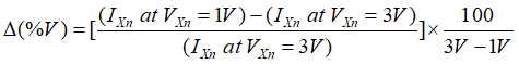
| ΔIREG(LINE) | Line regulation (R0-R15 / G0-G15 / B0-B15)(3) | VLED = 2.5 to 5.5V, All CHn = on, VOUTn = (VLED-1)V, at same color grouped outputs of R0-R15 / G0-G15 / B0-B15 | ±1 | %/V | ||
| ΔIREG(LOAD) | Load regulation (R0-R15 / G0-G15 / B0-B15)(4) | VOUTn = (VLED-1)V to (VLED-3)V, VR=VG/B=VLED=3.8V, All CHn = on, at same color grouped outputs of R0-R15 / G0-G15 / B0-B15 | ±1 | %/V | ||
| TTSD | Thermal shutdown threshold | 170 | °C | |||
| THYS | Thermal shutdown hysteresis | 15 | °C | |||
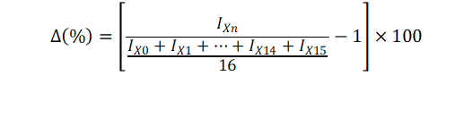
(1) The deviation of each output in same color group (OUTR0-15 or OUTG0-15 or OUTB0-15) from the average of same color group constant current. The deviation is calculated by the formula. (X = R or G or B, n = 0-15)
(2) The deviation of the average of constant-current in each color group from the
ideal constant-current value. (X = R or G or B):
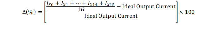 Ideal current is calculated by the following equation:
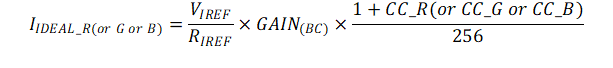
Ideal current is calculated by the following equation:
(3) Line regulation is calculated by the following equation. (X = R or G or B, n = 0-15):

(4) Load regulation is calculated by the following equation. (X = R or G or B, n = 0-15):