SNVSC61A August   2022  – December 2022 LP5891-Q1

PRODUCTION DATA  

  1. Features
  2. Applications
  3. Description
  4. Revision History
  5. Description (continued)
  6. Pin Configuration and Functions
  7. Specifications
    1. 7.1 Absolute Maximum Ratings
    2. 7.2 ESD Ratings
    3. 7.3 Recommended Operating Conditions
    4. 7.4 Thermal Information
    5. 7.5 Electrical Characteristics
    6. 7.6 Timing Requirements
    7. 7.7 Switching Characteristics
    8. 7.8 Typical Characteristics
  8. Detailed Description
    1. 8.1 Overview
    2. 8.2 Functional Block Diagram
    3. 8.3 Feature Description
      1. 8.3.1 Independent and Stackable Mode
        1. 8.3.1.1 Independent Mode
        2. 8.3.1.2 Stackable Mode
      2. 8.3.2 Current Setting
        1. 8.3.2.1 Brightness Control (BC) Function
        2. 8.3.2.2 Color Brightness Control (CC) Function
        3. 8.3.2.3 Choosing BC/CC for a Different Application
      3. 8.3.3 Frequency Multiplier
      4. 8.3.4 Line Transitioning Sequence
      5. 8.3.5 Protections and Diagnostics
        1. 8.3.5.1 Thermal Shutdown Protection
        2. 8.3.5.2 IREF Resistor Short Protection
        3. 8.3.5.3 LED Open Load Detection and Removal
          1. 8.3.5.3.1 LED Open Detection
          2. 8.3.5.3.2 Read LED Open Information
          3. 8.3.5.3.3 LED Open Caterpillar Removal
        4. 8.3.5.4 LED Short and Weak Short Circuitry Detection and Removal
          1. 8.3.5.4.1 LED Short/Weak Short Detection
          2. 8.3.5.4.2 Read LED Short Information
          3. 8.3.5.4.3 LSD Caterpillar Removal
    4. 8.4 Device Functional Modes
    5. 8.5 Continuous Clock Series Interface
      1. 8.5.1 Data Validity
      2. 8.5.2 CCSI Frame Format
      3. 8.5.3 Write Command
        1. 8.5.3.1 Chip Index Write Command
        2. 8.5.3.2 VSYNC Write Command
        3. 8.5.3.3 MPSM Write Command
        4. 8.5.3.4 Standby Clear and Enable Command
        5. 8.5.3.5 Soft_Reset Command
        6. 8.5.3.6 Data Write Command
      4. 8.5.4 Read Command
    6. 8.6 PWM Grayscale Control
      1. 8.6.1 Grayscale Data Storage and Display
        1. 8.6.1.1 Memory Structure Overview
        2. 8.6.1.2 Details of Memory Bank
        3. 8.6.1.3 Write a Frame Data into Memory Bank
      2. 8.6.2 PWM Control for Display
    7. 8.7 Register Maps
      1. 8.7.1  FC0
      2. 8.7.2  FC1
      3. 8.7.3  FC2
      4. 8.7.4  FC3
      5. 8.7.5  FC4
      6. 8.7.6  FC14
      7. 8.7.7  FC15
      8. 8.7.8  FC16
      9. 8.7.9  FC17
      10. 8.7.10 FC18
      11. 8.7.11 FC19
      12. 8.7.12 FC20
      13. 8.7.13 FC21
  9. Application and Implementation
    1. 9.1 Application Information
    2. 9.2 Typical Application
      1. 9.2.1 Design Requirements
        1. 9.2.1.1 System Structure
        2. 9.2.1.2 SCLK Frequency
        3. 9.2.1.3 Internal GCLK Frequency
        4. 9.2.1.4 Line Switch Time
        5. 9.2.1.5 Blank Time Removal
        6. 9.2.1.6 BC and CC
      2. 9.2.2 Detailed Design Procedure
        1. 9.2.2.1 Chip Index Command
        2. 9.2.2.2 FC Registers Settings
        3. 9.2.2.3 Grayscale Data Write
        4. 9.2.2.4 VSYNC Command
        5. 9.2.2.5 LED Open, Short Read
      3. 9.2.3 Application Curves
    3. 9.3 Power Supply Recommendations
    4. 9.4 Layout
      1. 9.4.1 Layout Guidelines
      2. 9.4.2 Layout Example
  10. 10Device and Documentation Support
    1. 10.1 Documentation Support
      1. 10.1.1 Related Documentation
    2. 10.2 Receiving Notification of Documentation Updates
    3. 10.3 Support Resources
    4. 10.4 Trademarks
    5. 10.5 Electrostatic Discharge Caution
    6. 10.6 Glossary
  11. 11Mechanical, Packaging, and Orderable Information

Package Options

Mechanical Data (Package|Pins)
Thermal pad, mechanical data (Package|Pins)
Orderable Information

Grayscale Data Write

The channel grayscale data is written to SRAM of the device by the data write command with non-broadcast way, details can be found in Data Write Command and Write a Frame Data into Memory Book.

Data Write Flow is the data write flow for this application, P (i, j) is the data of pixel locating in I + 1 row and j + 1 column. Suppose channel R15/G15/B15 of each device is not used and not connected, the channel R14/G14/B14 is connected to P(i, 0), the channel R13/G13/B13 is connected to P (i, 1),…, and channel R0/G0/B0 is connected to P (i, 14). The data of unused channel must be zero noting D_Zero in below figure, and D_Zero = 00000000000000001 00000000000000001 00000000000000001b.
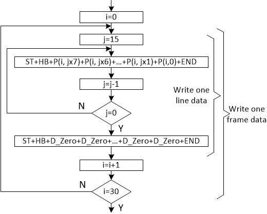
GUID-0D5175CC-0353-43F4-B8EE-5364D349E86C-low.gifFigure 9-4 Data Write Flow